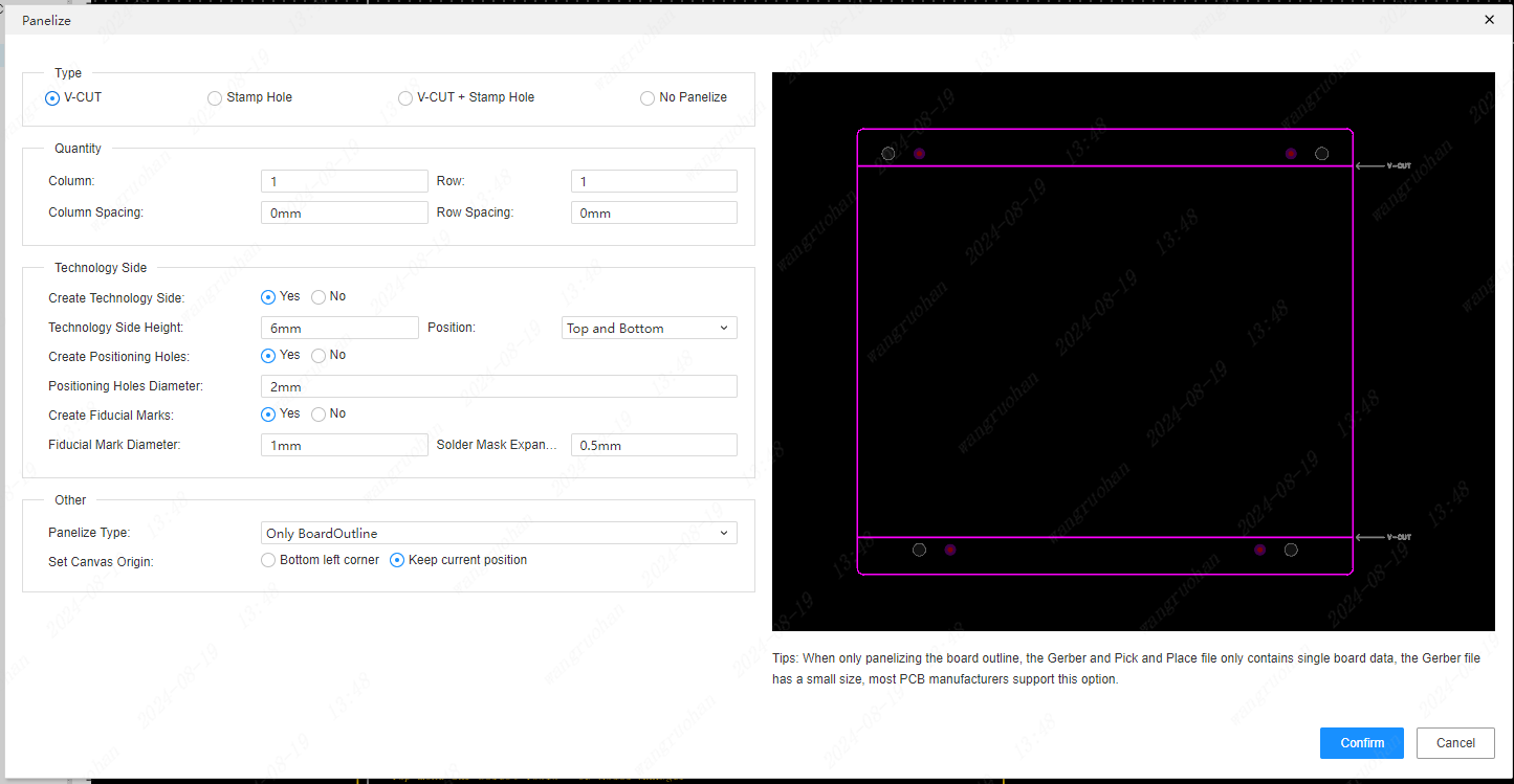
Panelize
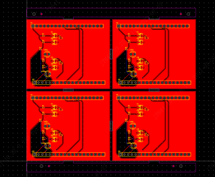
EasyEDA provides a powerful patchwork function, it can be very convenient for the patchwork operation. The assembling function provided by the editor only supports the assembling of the current board, and does not support the assembling of multiple different boards. To assemble multiple different boards, you need to use the manual assembling function.
Panelize
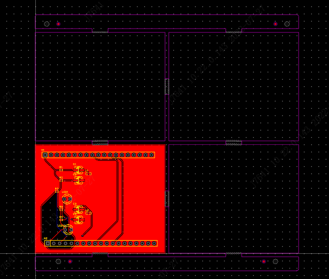
After the PCB is drawn, make sure that the border of the board has been drawn and closed, you can use the board assembling function.
Entry: Top menu - Tools - Panelize
No Panelize
The parameters of the jigsaw are saved in the file. If the jigsaw is not needed, select not to jigsaw
Type of board
V-CUT Panelize :
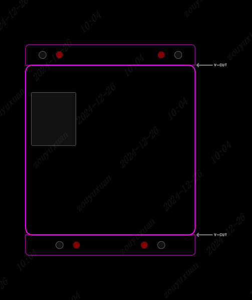
According to the design of the board, the V-cut board is adopted. When assembling the board, the array will be generated according to the border/board frame, and then the panel preview will be generated according to the other parameters set.
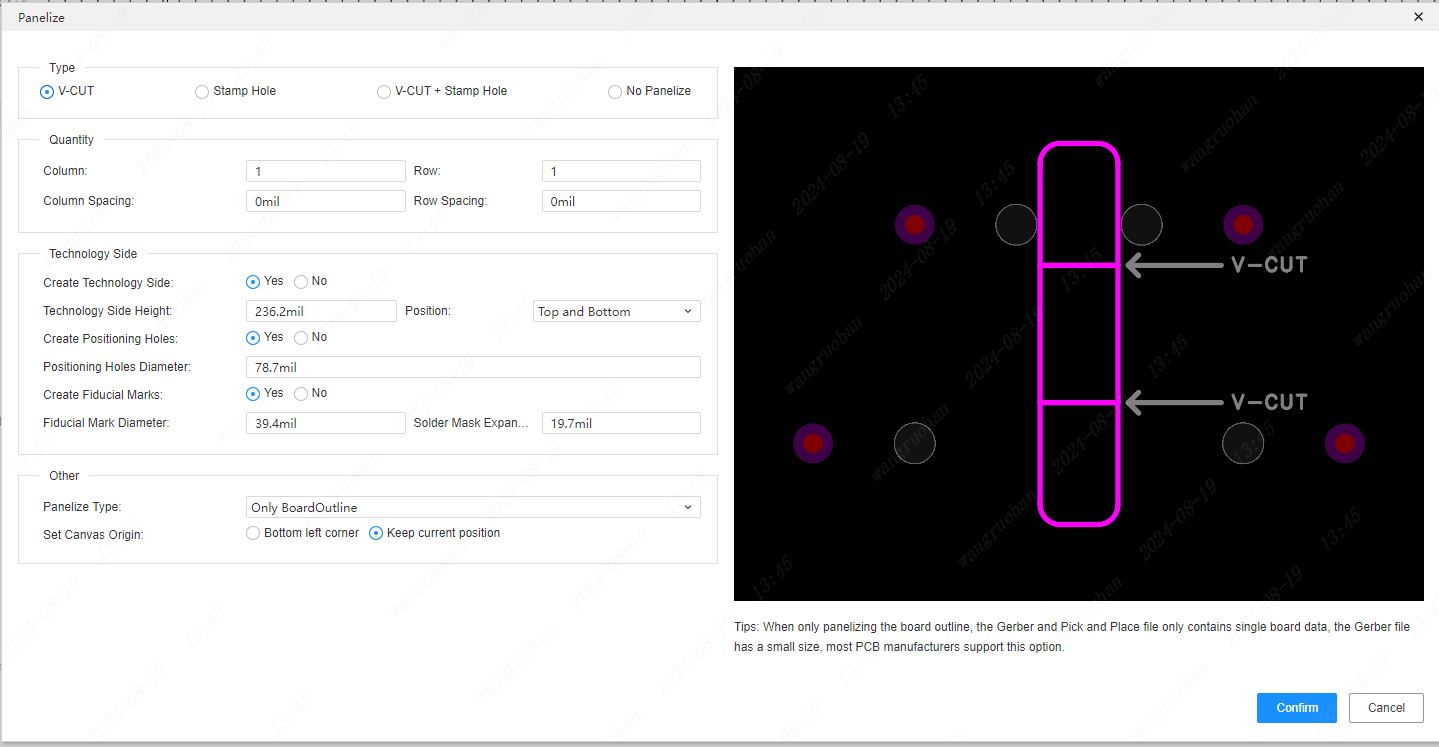
In production, it will cut V according to the border line, and cut a fine groove to the V-shape of the board. After completion, it is necessary to manually break off the separation board.
Stamp Hole Panelize :
Stamp hole plate is through multiple groups of through the hole, the need to join the board together, after the production is finished, the link is broken manually.
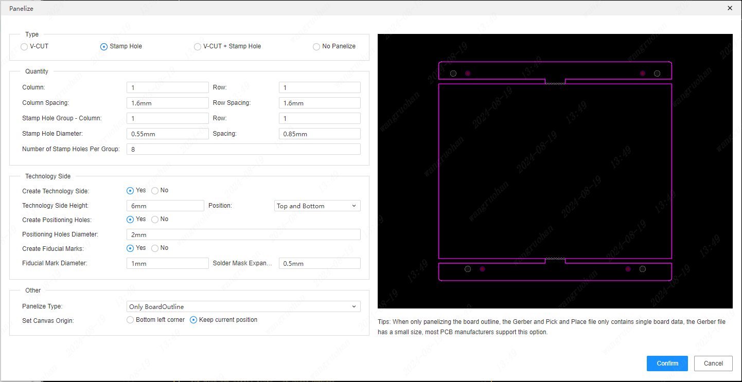
The number and size of the stamp holes can be set according to the need
V Cut + Stamp Hole Panelize :
V cut and stamp hole combination plate, more suitable for irregular shape board, and devices need to highlight the board frame scene.
Technology Edge
Support setting process edge height and positioning hole and anchor point (MARK point) size.
Process edge is usually used for SMT placement when the board enters the placement track, and also facilitates SMT placement positioning. You do not need this option if you are working on the JLCPCB patch.
Other Options
The Panelize mode supports two types:
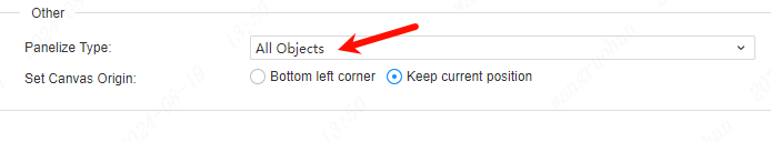
Only spell borders. This method is recommended. When only bounding frame is assembled, 2D and 3D preview, Gerber and coordinate files only include board data. Gerber files are small, and most board manufacturers support this assembling method. Calicron supports this approach.
Concatenate all objects. When splicing all pixels, Gerber and coordinate files contain all board data. Gerber files are large, and some board manufacturers need this method.
Manual Panelize
When automatic assembling cannot meet the needs, such as the need to assemble different boards, Yin and Yang assembling (such as Tai chi graphics), manual assembling can only be used.
It should be noted that if the PCB of manual assembling is too large, it will lead to PCB stalling and difficult alignment, so it is recommended to use the automatic assembling function.
Steps:
- Open the PCB that needs to be assembled, or other different PCB
2, box select or CTRL+A select all PCB contents, CTRL+C copy
- Switch to the PCB that needs to be assembled, CTRL+SHIFT+V paste. The shortcut paste will automatically hide the flyline layer and the hold bit will not increase.
4, you can paste when the point, or placed after the batch box to choose the point, you can also put the board combination after moving the point.
5, if you need the process edge and V secant, then draw the border line in the border layer (plate and frame layer).
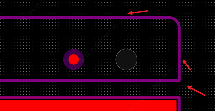
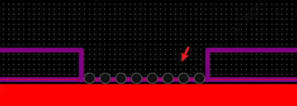
6, if you need a stamp hole, place a circular grooved area, set the size and spacing, on the border line. The diameter of the stamp hole is 0.55mm, and the spacing is 0.85mm
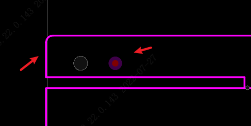
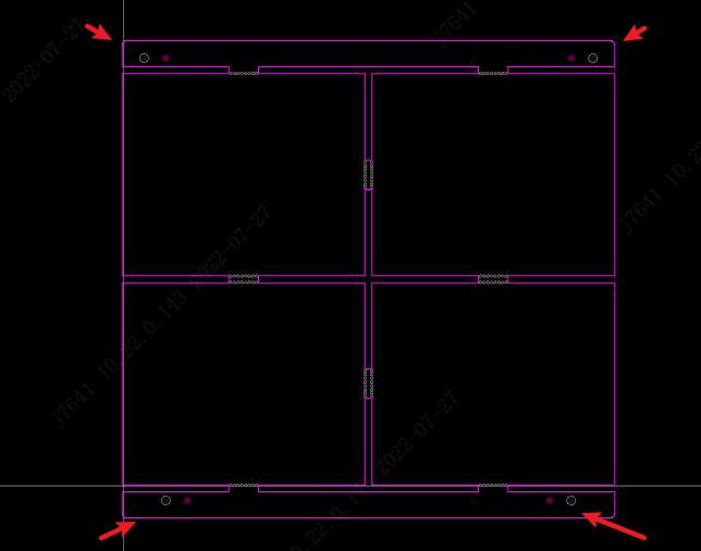
- If positioning holes and positioning points are needed, circular grooving areas (positioning holes) can be placed, and single-layer solder pads (positioning points) can be added. The positioning point shall be placed on both the top and bottom signal layers. The diameter of the positioning hole is 2mm, the diameter of the positioning spot welding plate is 1mm, and the welding resistance extension is 0.5mm.
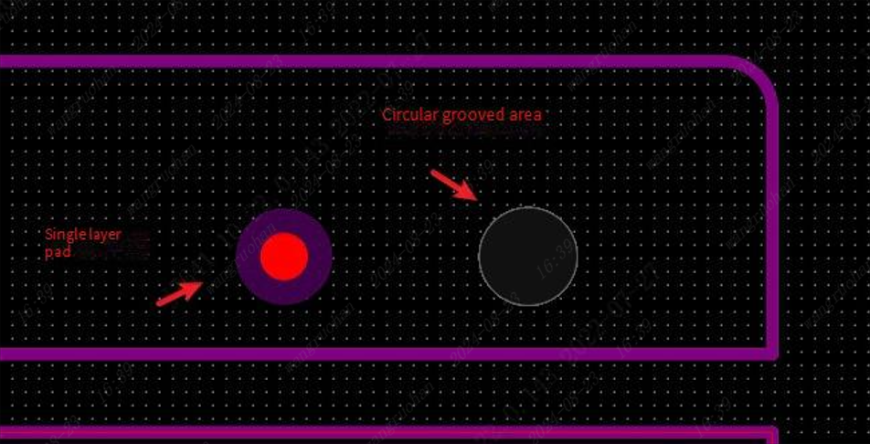
The positioning holes and positioning points need to be placed diagonally, and the distance between the upper and lower sides and the left and right boundaries should not be the same, otherwise the SMT cannot be accurately located, as shown in the figure.
Notice:
- The board with an internal plane layer cannot be used by manual panels, otherwise the inner electric layer cannot take effect normally.Because the implementation method of the internal plane layer must be available with the full border, manually copying and paste multiple borders in the border's internal plane blocks will be abnormal, and the network cannot inherit. It is necessary to change to the signal layer with copper instead of internal electricity segmentation.
- The editor's own panel and manual panel cannot be performed at the same time.
- Supports copying the slot Region to the collage in the Panelize Type of Only BoardOutline