Update Place and Route From Reuse Template
The professional version of easyEDA pro a reuse module function. Through this function, the PCB can be reused to achieve the purpose of layout wiring reuse.
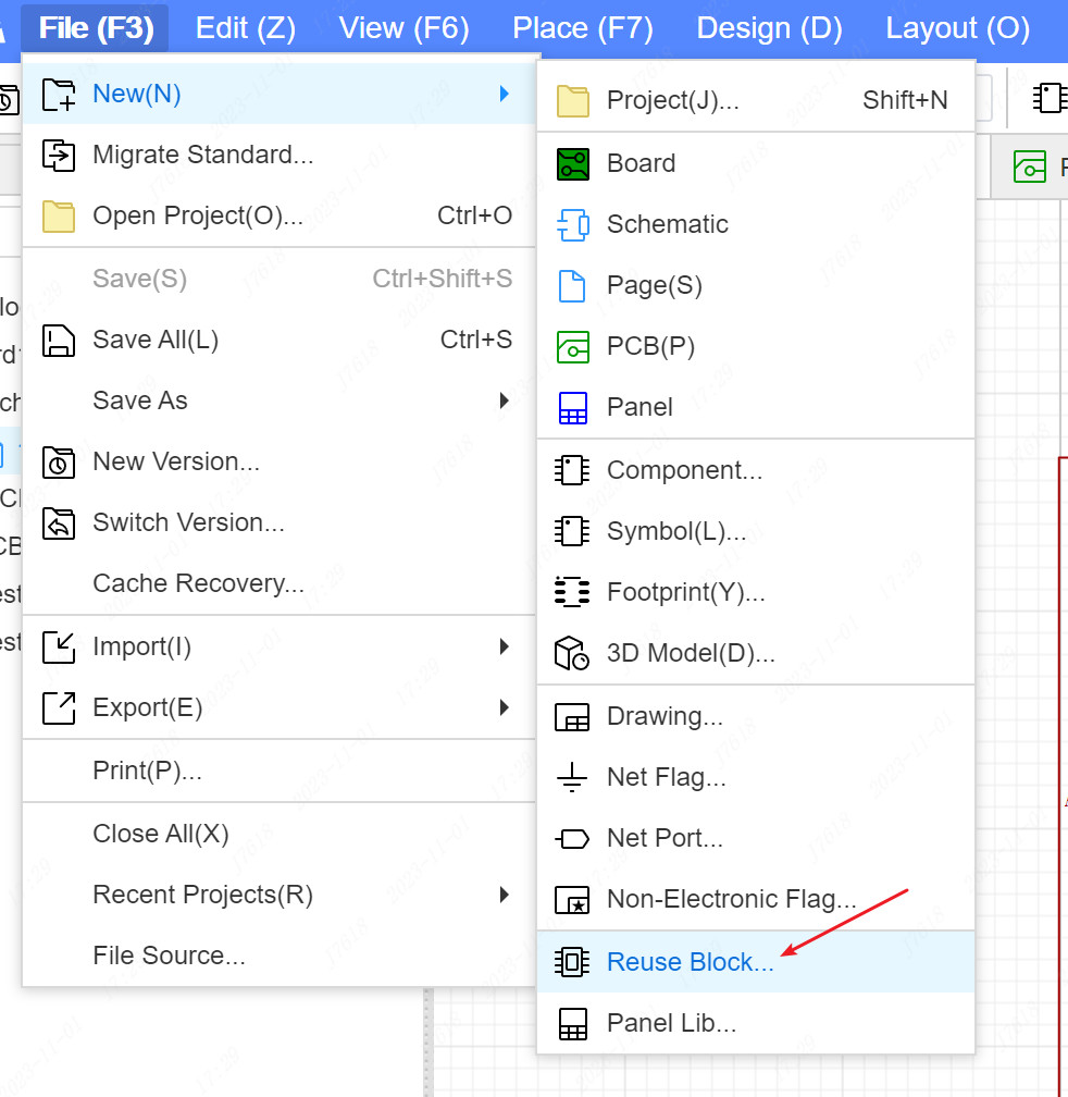
Create reuse block
- Steps: top menu - file - new - new - reuse block
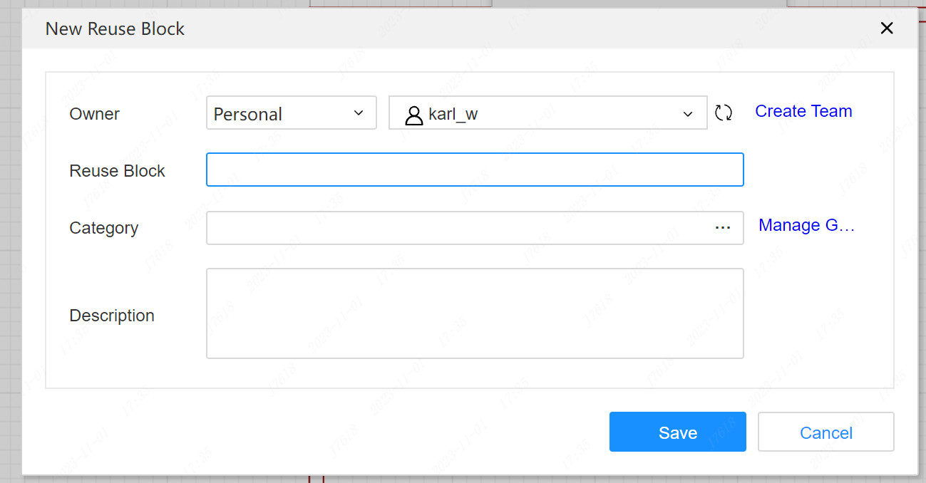
The reuse block is a special project that will be stored in the reuse module library. When newly built, the module can be set to classify and describe it.
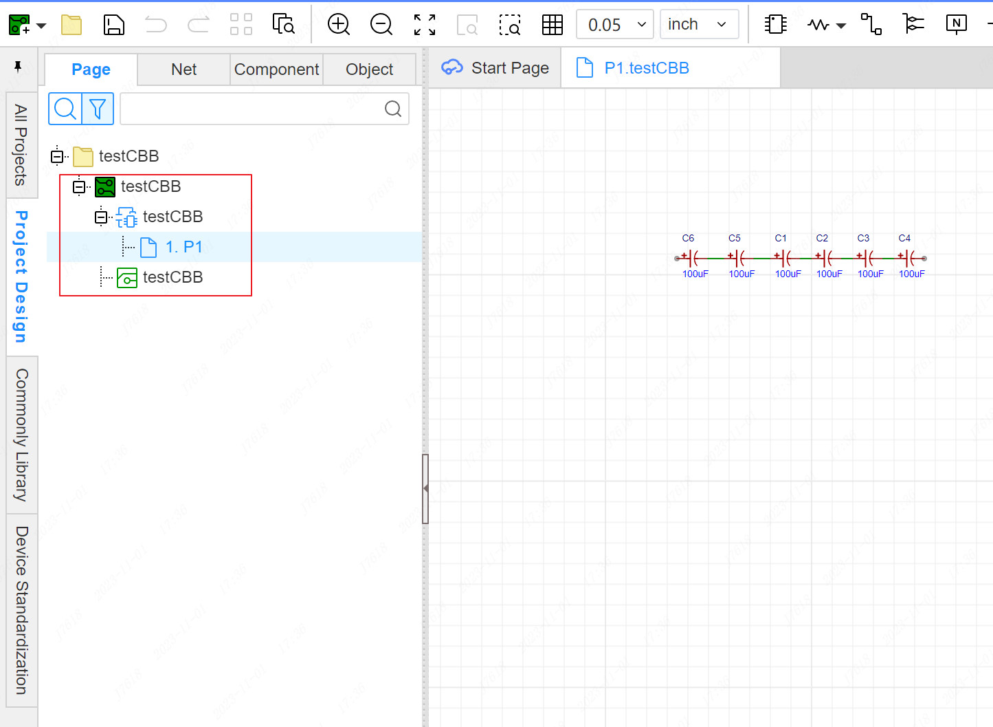
After the successful creation of the reused module, it will create a board that contains schemes and PCB under the project by default, a symbol.
Notice:The principle diagram, PCB, and symbols are associated through the name. If the names of a certain type of type are modified separately, they will be disconnected between them when quoting, and they cannot be reused together.
In the module engineering, the principle diagram and PCB are designed. Before saving, you can click the schematic diagram to the PCB again.If you need to reference the schematic diagram in a symbol, keep the pin of the symbol with the name and number of the network port of the schematic map page consistent, and you can view the reuse block-create a reuse block.
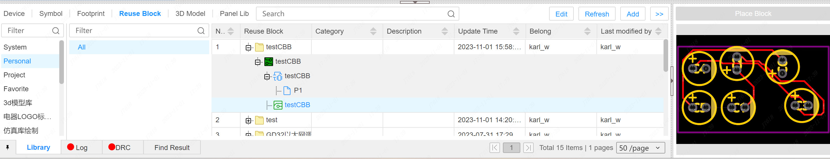
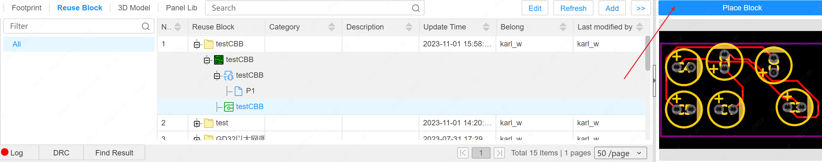
Place the reuse block
- Steps:The bottom panel - library - reuse block
After placing the reuse block in the schematic diagram, transfer to the PCB, the PCB will automatically form a module based on the layout of the layout in the reuse module; it can also be directly placed in the PCB, but this method is placed in the schematic diagram and the PCB network.The table is not associated.
Schmatic Place
In the schematic diagram, you can directly place the reuse module, which are divided into two methods: symbolic method and combined method. These two methods will be displayed in the schematic graphic cloth, but when transferring to PCB, you can use it to the PCB, you can use it to the PCB.The entire PCB module is combined together to avoid re -layout of wiring operations and improve design efficiency.
During the placement, the page of the pages of the left panel will automatically create the schematic diagram and PCB template under the reuse module project. The subsequent schematic diagram to PCB and the layout of the renewal template will be reused from this template.
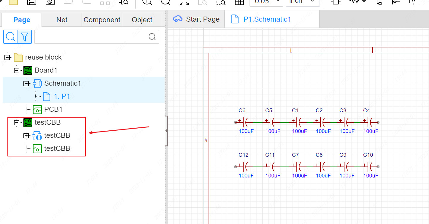
After the schematic diagram is placed, the different forms of different forms generated in the schematic diagram, please check in the reuse module-place the reuse module chapter.
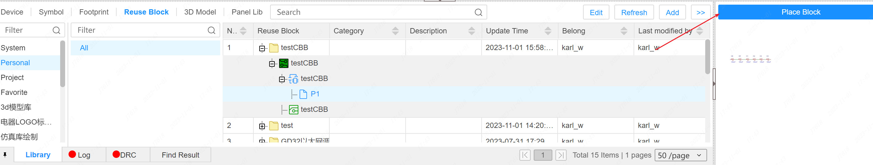
PCB Place
The PCB under the module library in the PCB can also directly place the module. After clicking
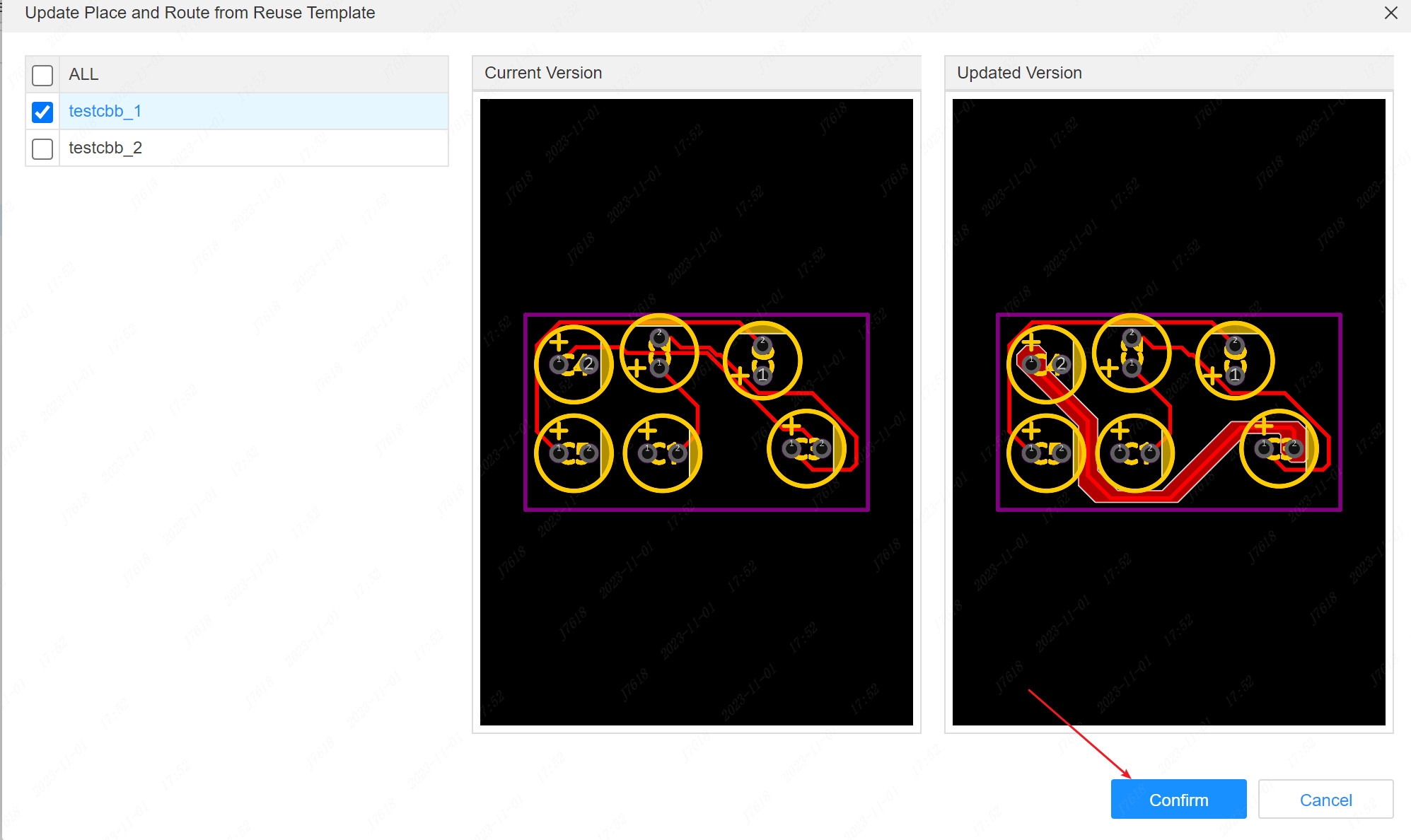
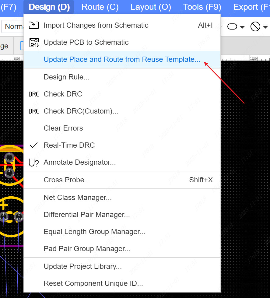
Update Place and Route From Reuse Template
After the layout of the PCB module is updated, it is very troublesome to modify it separately in each module in a PCB.PCB templates once, and then update to all the current PCB citations.
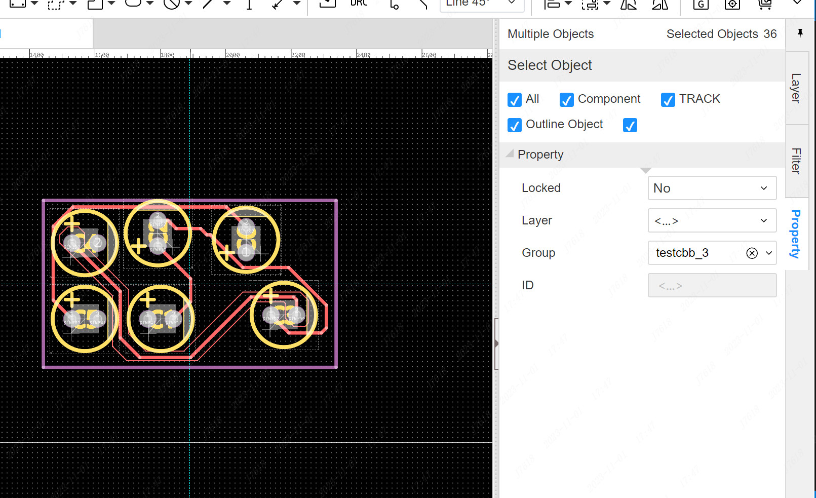
Reuse block properties
After the principle diagram and PCB are placed, each component in the module automatically generates the attributes related to the reuse module, which is used for the follow -up schematic diagram to the PCB automatic layout wiring and update the layout wiring from the template.
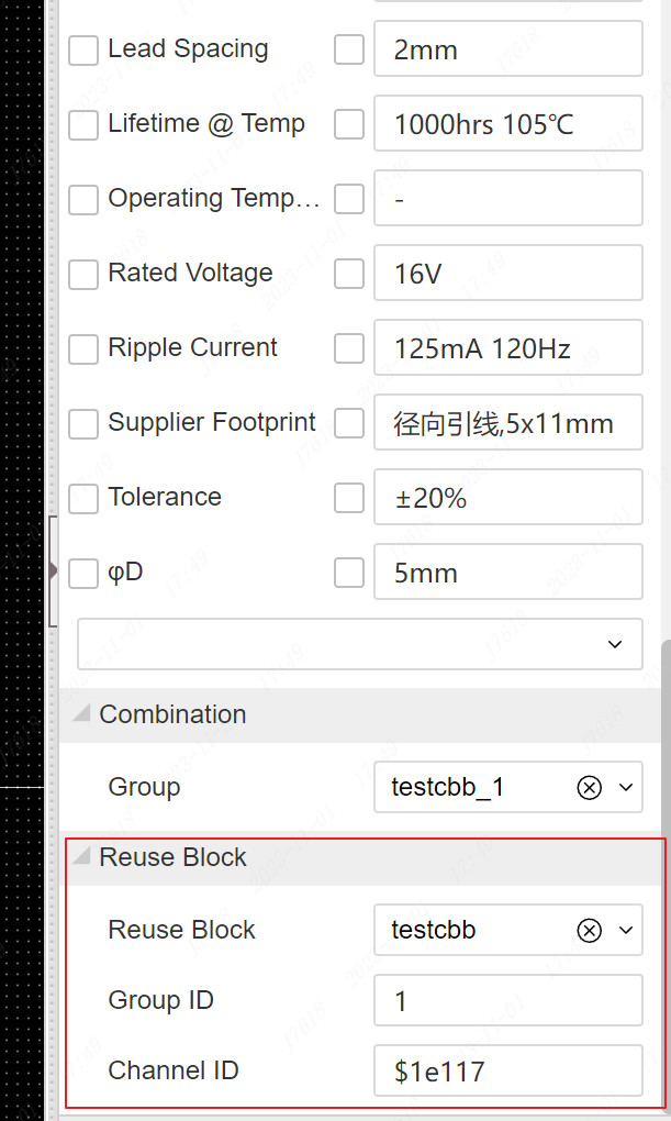
Reuse block: The component with the same name of the reused block belongs to a template. The PCB of the same name in the left map tree is their template PCB
Group ID: One module may be repeatedly used, and multiple groups will be generated. The group ID attribute is used to distinguish the current component belongs to that group
Channel ID: There may be components that may be encapsulated by multiple same devices in a module. The channel ID is used to confirm the specific location of the component in the module
Update from template
Steps:Top Menu -Design -Reproduce template update layout wiring
From the pop -up layout of the reuse template, the list of the module+group ID of the module+group ID is listed on the launch of the layout layout. Select the corresponding module. You can preview the difference between the current version and the latest version of the template on the right side
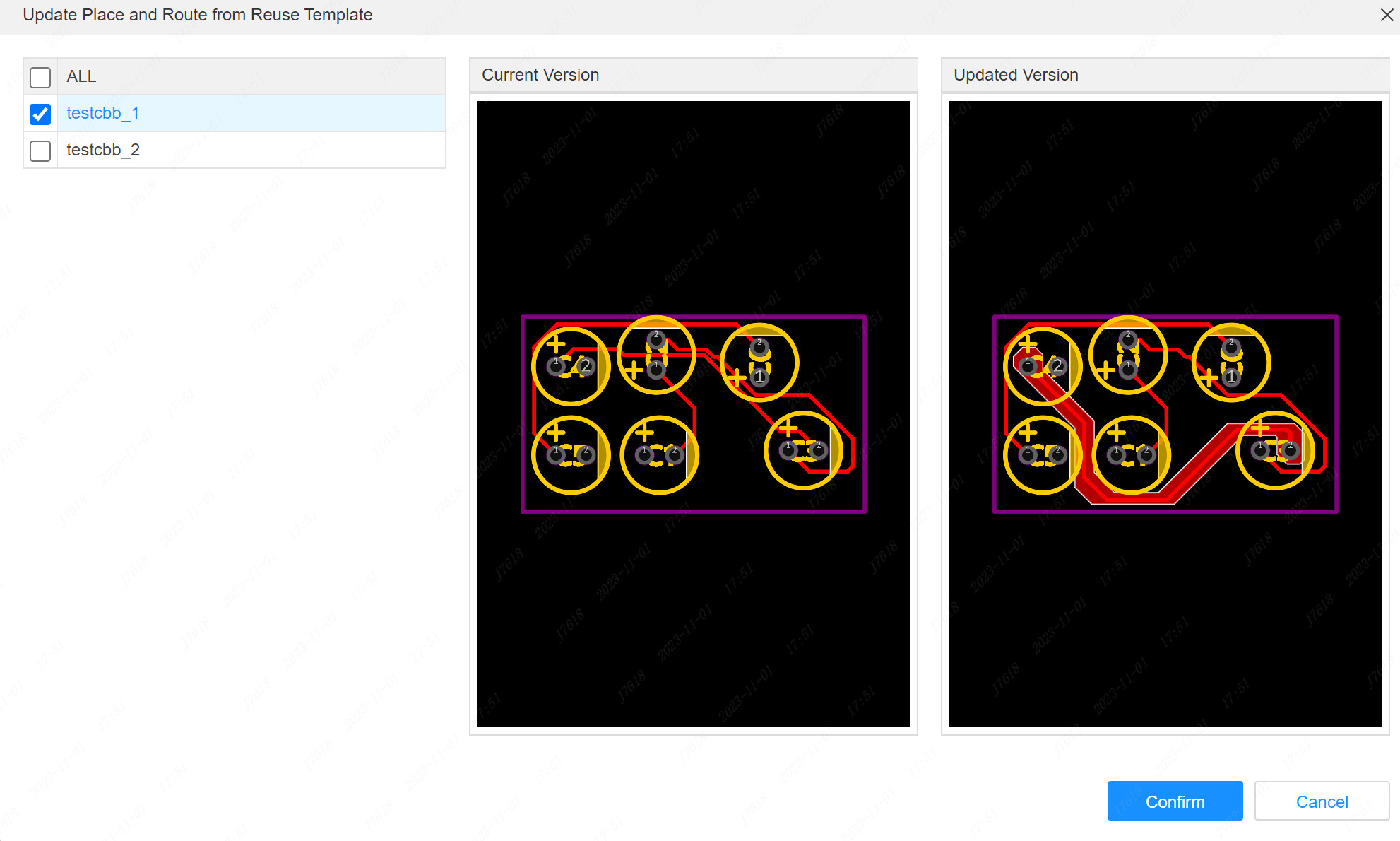
Check the module that needs to be updated. Click to confirm that the corresponding module in the canvas will re -lay back to the latest template to lay out the wiring.