Schematic FAQ
Component designator assignment for reused blocks
Details
In the top menu - Design - Annotate Designator, assign component designators 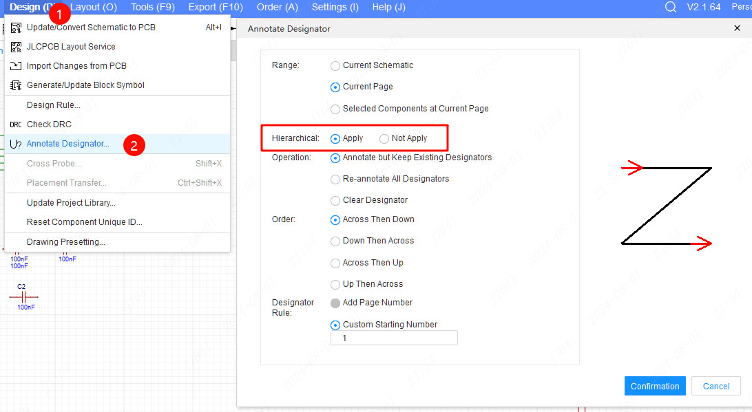
or you can expand the reuse block symbol to go to Hierarchical schematic to annotate the designator 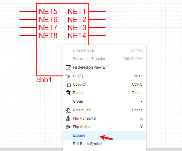
According to the above operation, the component designators in the reuse module can be completed.
How to move all components to the grid points
Details
Schematic grid alignment
Click or select the component, press the shortcut key CTRL+SHIFT+G
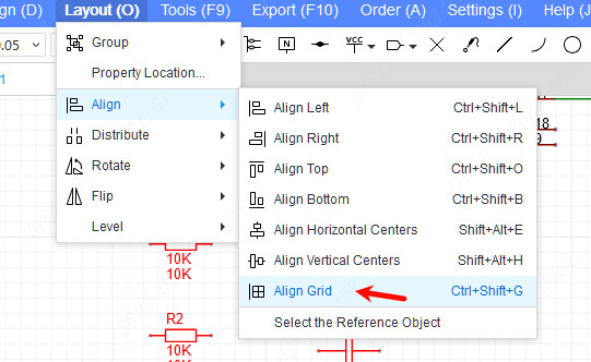
PCB grid alignment is also operating
How to edit symbols in schematics
Details
You can select a component, and right-click it and use "Edit Device", if you use "Symbol Management Mode" is profession mode, you can use "Edit Symbol". 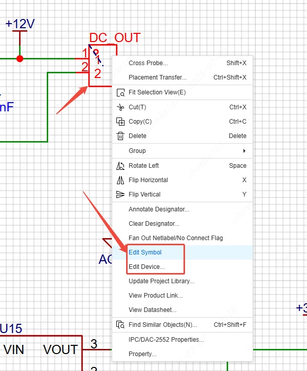
How to edit drawing or sheet symbol style and content
Details
You can click the edit icon to edit the drawing symbol 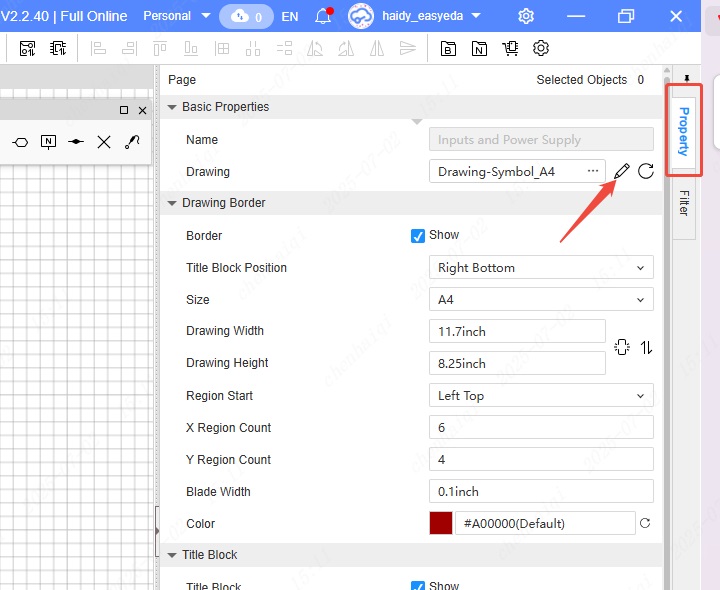
the more info please refer at Drawing Symbols
How to switch units in schematics
Details
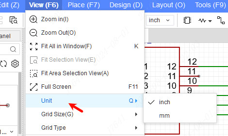
In the top menu bar, currently supports inch and mm unit switching
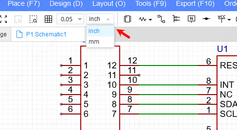
or you can change unit at View menu
How to modify the size of the drawing
Details
In the properties panel on the right, click "Drawing Symbols" and select other sizes of drawing symbols.
Specific reference.
Project Drawing Setting:https://prodocs.easyeda.com/en/schematic/design-project-drawing-setting/index.html
Drawing Symbol Creation:https://prodocs.easyeda.com/en/symbol/file-new-symbol-drawing-symbol/index.html
How come my updated library is still old when I place it again?
Details
EasyEDA Pro Professional supports the concept of a project library. The placed library will automatically enter the project library as a template, and the next time you place a library from the same source will give priority to the template inside the project library, avoiding the update of individual libraries to affect the existing design of the project.
The project library can be edited, the entrance is: bottom panel - Component Library - Project - Device/Symbol/Footprint.
You can also update the project library directly, the entrance is: Top Menu - Design - Update Symbols/Devices
Please refer:https://prodocs.easyeda.com/en/schematic/side-bottom-panel-project-library/index.html
How to place net labels
Details
EasyEDA Pro Professional no longer supports separate net labels like the standard version, the Professional version's Place net labels (shortcut N) actually automatically sets the name for the wire. Please draw the wire and then set a name attribute to the wire, the wire name is the network name. You can also create a network by placing a net labels one the wire. 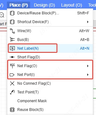
How to create a hierarchy schematic
Details
In the top menu - Place - Reuse Blocks, enter the name of the block, when finished, right click on the selected block and expand it, at this time you can place ports, device symbols, etc. Then create the pin information of the Reuse block symbols, etc. by using the: Top menu - Design - Update Block Symbols. After creation, you can switch to the project library in the bottom panel (shortcut S to open) and switch to the Reuse blocks for Place in the schematic.
Multi-level nested hierarchical diagrams can be supported.
How to batch rotate the circuit
Details
When the batch selection circuit has included wires, the whole rotation is not allowed. Press the space bar to rotate when the wires are not included.
How to create multiple sub projects in a project
Details
In the top menu - New - Board, a new board, schematic, PCB will be created automatically, at which point multiple board designs can be supported. 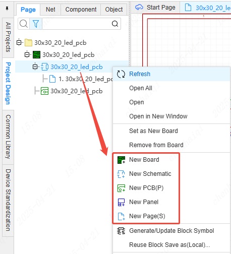
How to set components not to update to pcb?
Details
Select the component in the schematic and then modify the properties in the properties column on the right.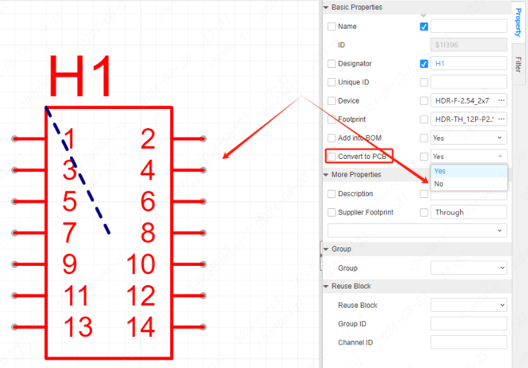
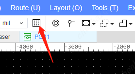
How to set the canvas grid display type for schematic and pcb?
Details
Adjustments can be made in the top menu bar.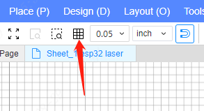
How to show or hide the pin numbers of a device in the schematic?
Details
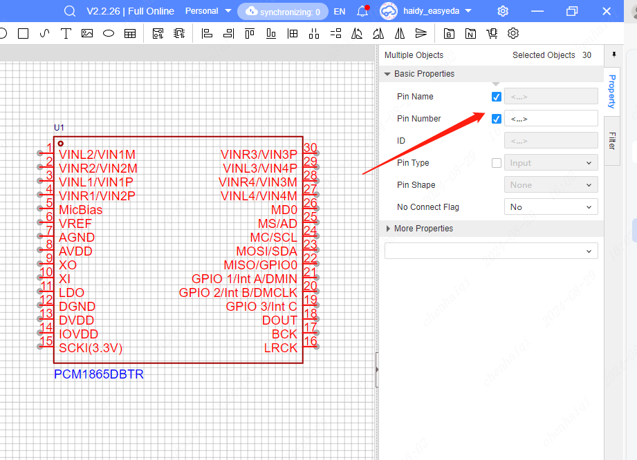
Firstly, you need to tick pin separately inside the filter panel. Then use the box-select function to select multiple or individual devices, and tick them off in the right-hand properties column after they are selected.You can also achieve the effect of batch processing.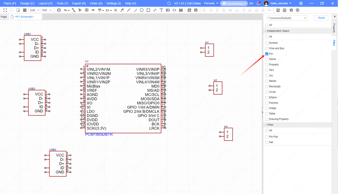
How to merge the two schemes into one schematic diagram?
Details
You just need to use the shortcut "ctrl+c" and "ctrl+v" to copy and paste to achieve the effect.This method also applies to merging pcb's at the same time.
How to deal with when a schematic diagram appears purple dotted line?
Details
The dotted purple line indicates that the symbol was recently modified and needs to be updated. 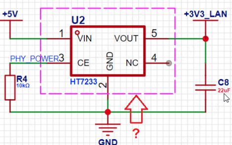
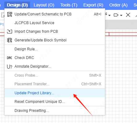
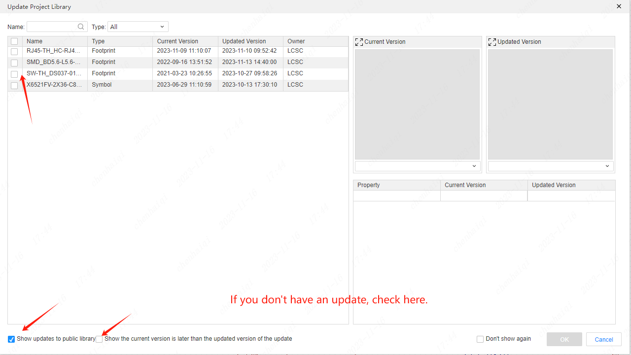
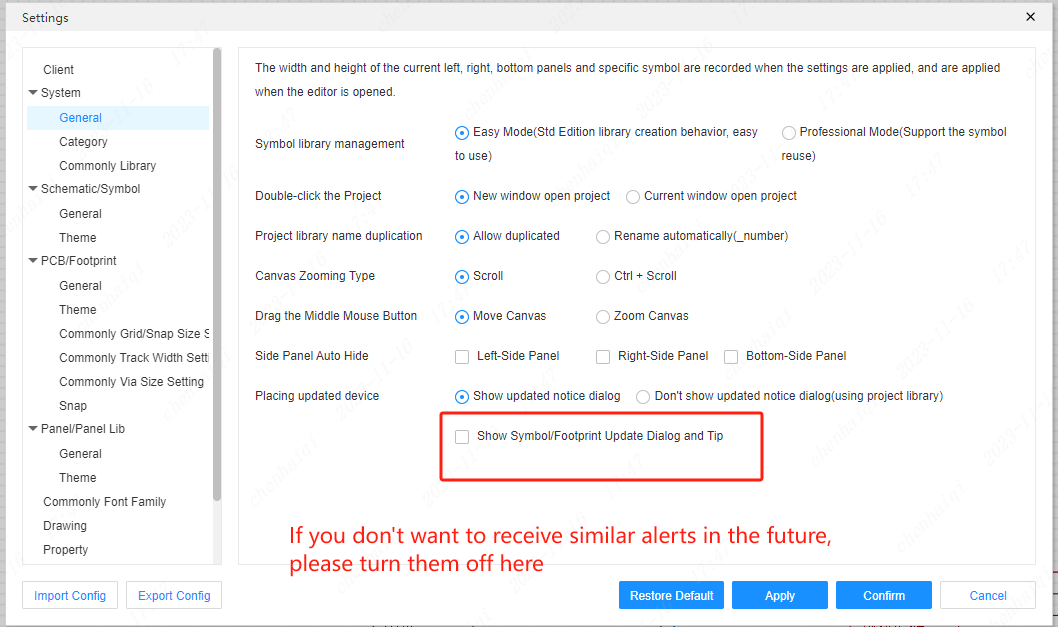
How to use the Find and Replace function to customize the allocation of Designator?
Details
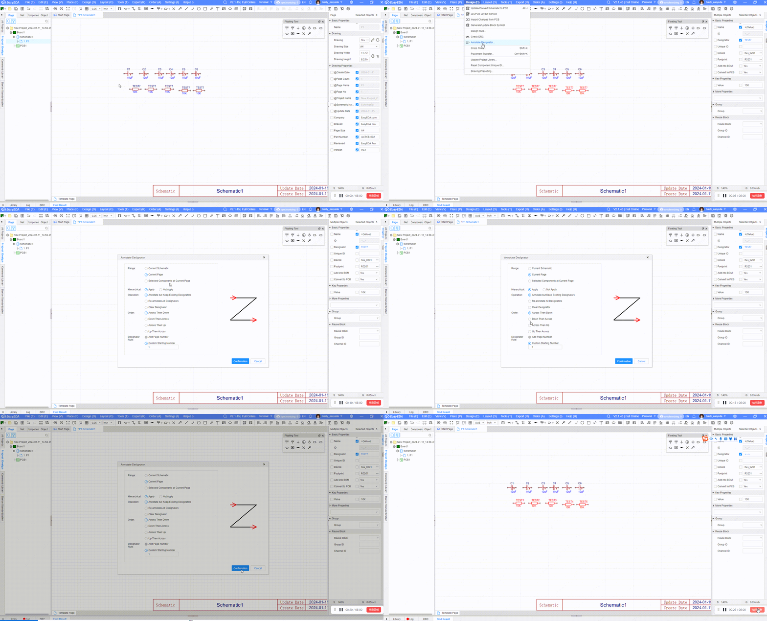
Step 1: In the top menu bar to Find "the Find and Replace function". Step 2: Select and input relevant search information. Step 3: Select the replacement function and input the prefix to be replaced.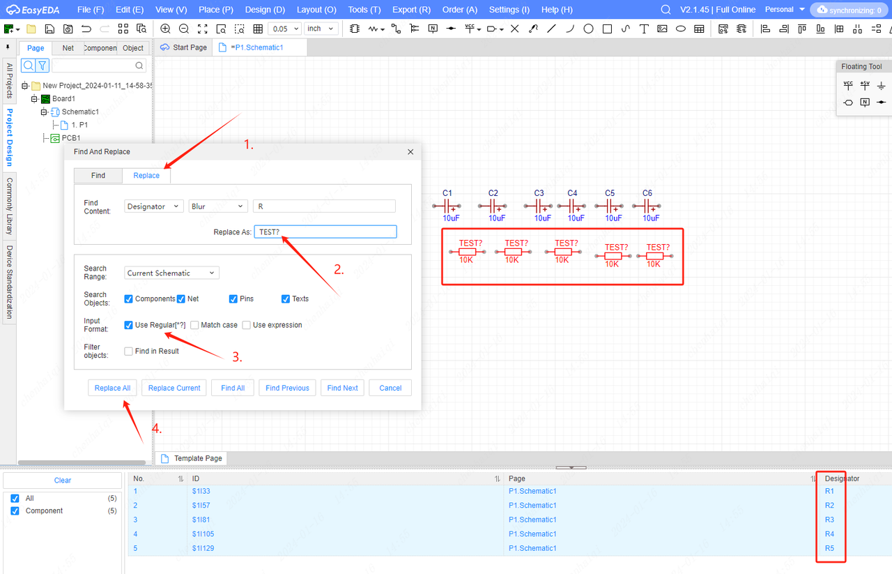 Step 4: Select "Annotate Designator" in the top menu bar and then reallocate.
How to plot a curve in a schematic?
Details
The tool ‘Bezier’ for drawing curves can be found in the top menu bar under ‘place’.Note that curves cannot be used as wires to connect pins. 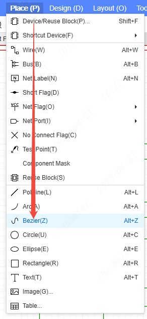
How to resolve the "Component properties does not match the supplier part" error?
Details
 This is because the official library attributes of eda have been updated. We can replace components by using the device manager function.Please refer:https://prodocs.easyeda.com/en/schematic/tools-device-manager/#device-manager
How to change the background color of the pcb and schematic?
Details
Select ‘Schematic/Symbol’ from ‘Settings’ in the top menu bar to enter the ‘Theme ‘Setting, you can modify the canvas color of the schematic as well as the colors of other settings. 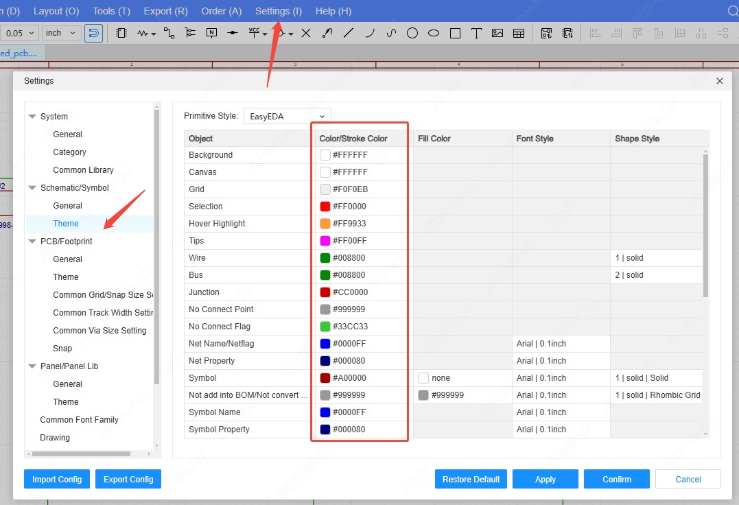
How are the pins of a symbol set to be Active-low?
Details
Add "~" before the network name. 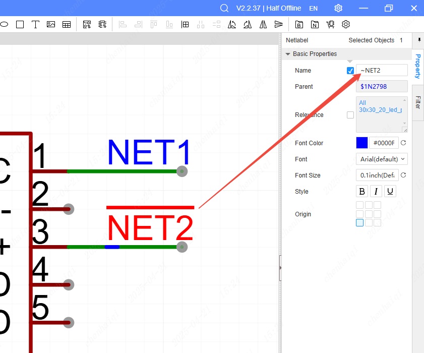
How to show and hide the Designator of a device?
Details
In the schematic, you can select the device first, then find the corresponding element box in the right property bar and choose to check Show Attributes and Uncheck Hidden Attributes. 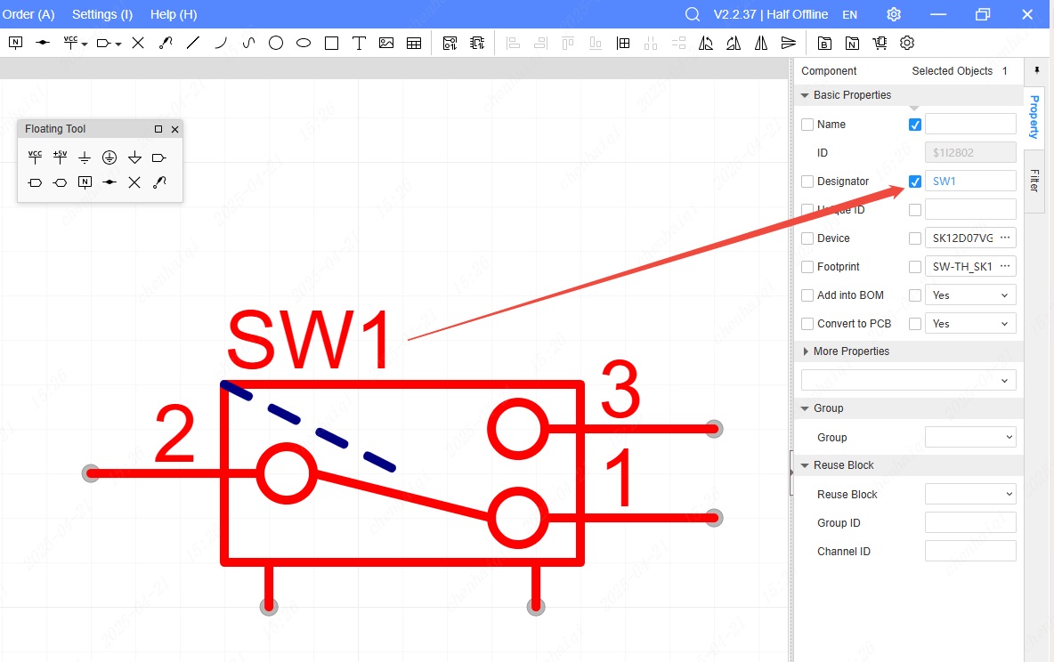
How to place network labels in bulk based on pin names?
Details
Step 1: Select the device, click the right mouse button and select the “Fan Out Netlabel/No Connect Flag” function. Step 2: Select the pin you want to operate. Step 3: Click on “Fill in the pin name with the net name”Function and you can click on Confirm once the network name is displayed.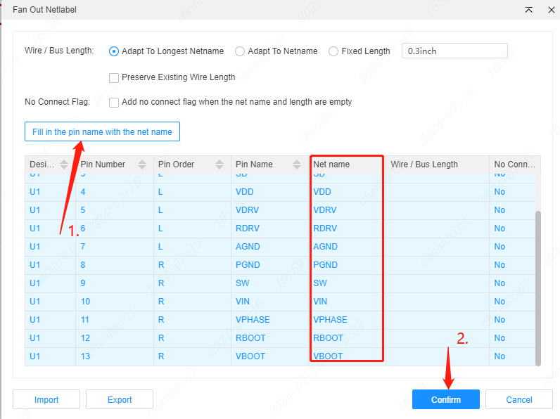
How to set the device not to be added to the bom file?
Details
Select the device, and in the right property column you can modify whether you need to add bom or not. 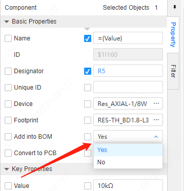
How does the netlist compare function work?
Details
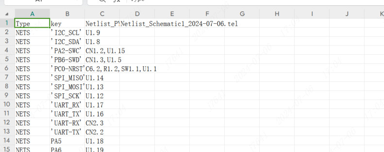
Starting from version 2.2, there is a ‘Netlist Compare’ entry on the start page of the editor, which allows you to load two netlist files and compare them to get the netlist differences, which will be exported in an xlsx table. This feature can be used to view the netlist differences of a schematic after format conversion or between two different versions of the schematic. Multiple EDA netlist formats can be supported. 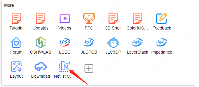 It is able to support allegro's tel format, zuken's ccf format, Altium's net format, PADS' asc and txt formats, and easyeda's enet format files. After selecting two netlist to import, it will automatically compare and export an xlsx file, which can be opened to view the pin differences of each network.
What is the difference between the symbol library Easy Mode and Professional Mode?
Details
You can change the mode in Settings General on the top menu bar. 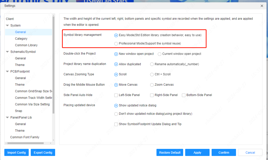
The difference is: When creating a new component in Easy Mode, only the component will be displayed. The bottom panel only displays the component toolbar. When you create a new component in Professional Mode, it will show the creation of components and symbols. 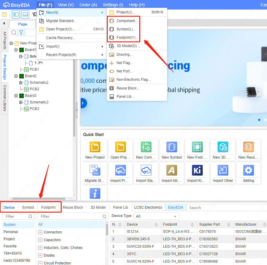
How to automatically display property values when placing a device?
Details
Go to the Settings toolbar in the top menu bar, and then select the Properties function to modify the settings. 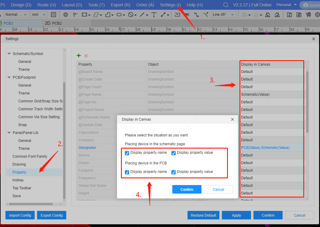
How to set up automatic adjustment of attribute positions when rotating symbols?
Details
Go to the Settings toolbar in the top menu bar to find the Schematic General tool and tick the corresponding function settings. 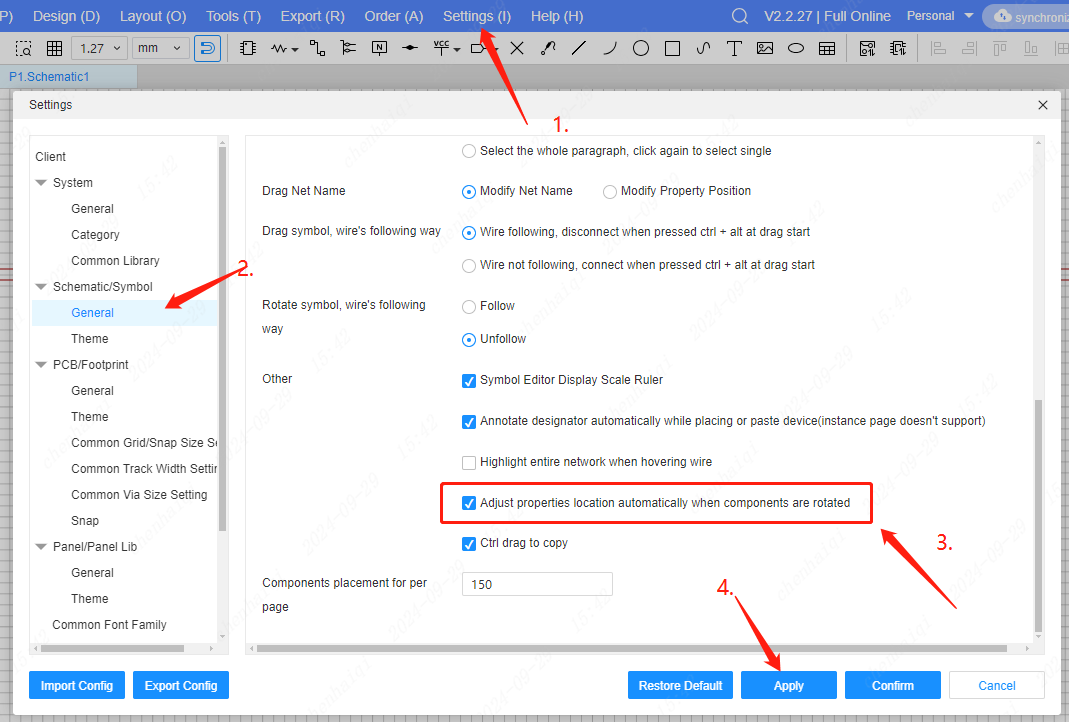
How do I place multiple numbers on the pins of a symbol?
Details
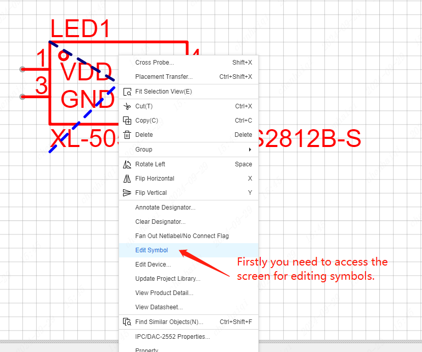
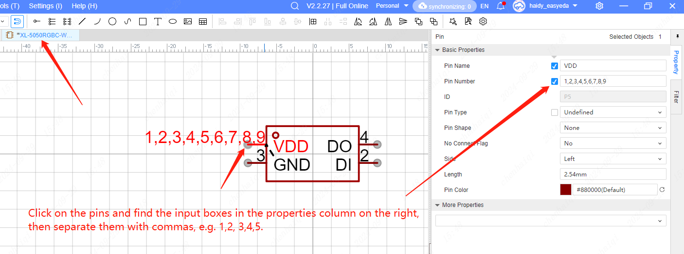
What can I do if the system prompts for a schematic page with more than 150 components?
Details
First of all, you can first check how many components there are on each page in the Objects side of the left menu bar, and then delete them according to the design. 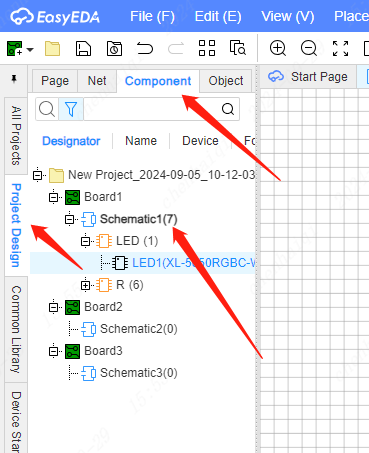
Or, in the Settings toolbar on the top menu bar, change the number of components allowed per page in the Schematic General Settings to the number you want. 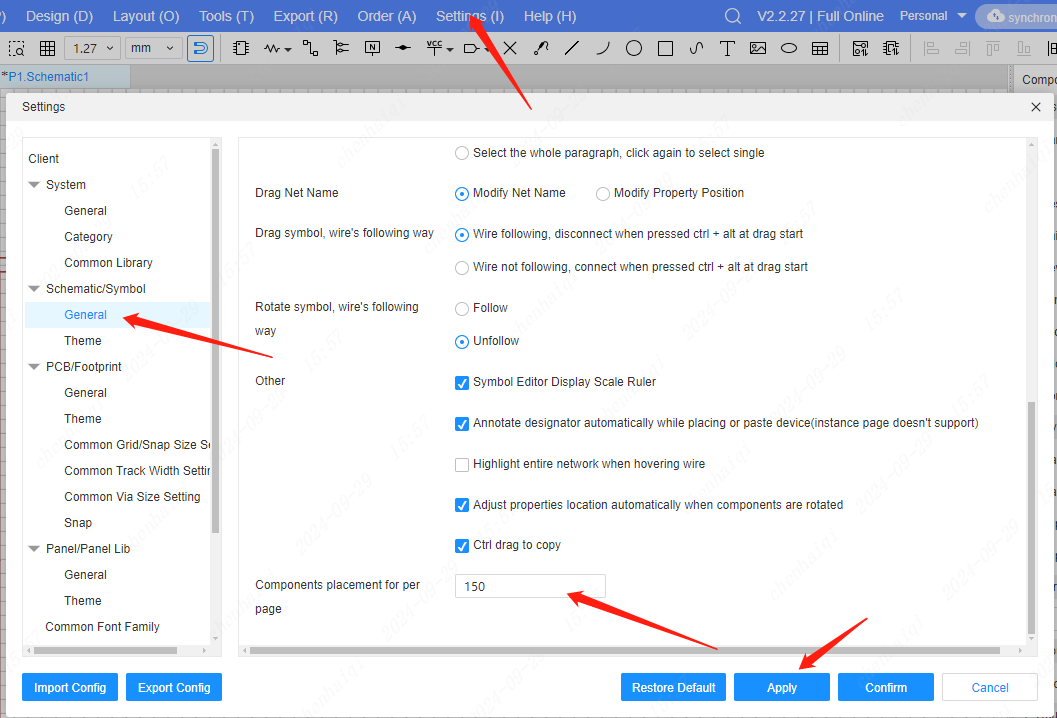
How to set whether Designator is retained when placing or copying and pasting?
Details
Both the schematic and PCB screens can be set to change the function. It can be found inside the Setup Tools in the top menu bar. 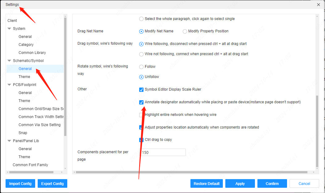
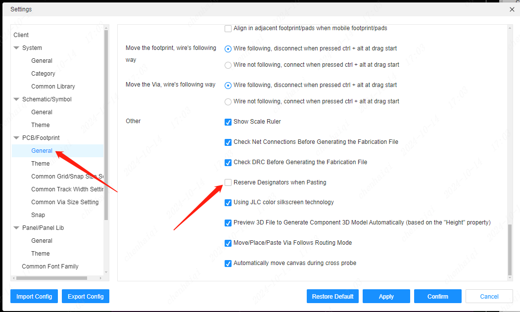
How does the schematic cancel the snap?
Details
You can set it in the Setup tool in the top menu bar, or you can use the hotkey ‘ALT+S’. 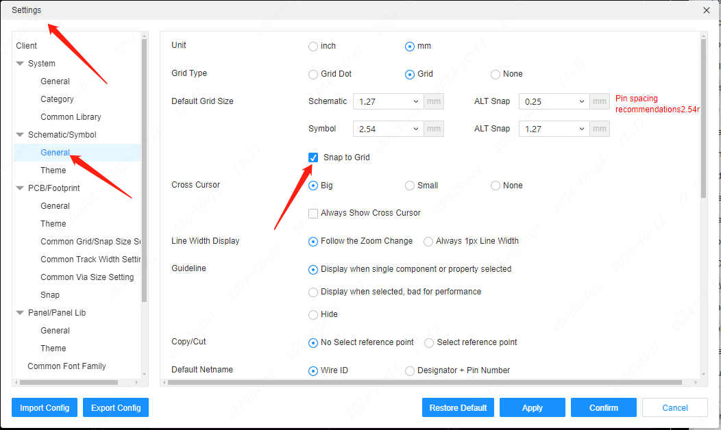
How to draw the wires in the schematic to get the red nodes?
Details
The red nodes are actually intersection points, indicating that the two wires intersect.So all we need to do is click where we need to intersect when we draw the wires to get the intersection point. 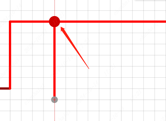
How to check how many pins the schematic has?
Details
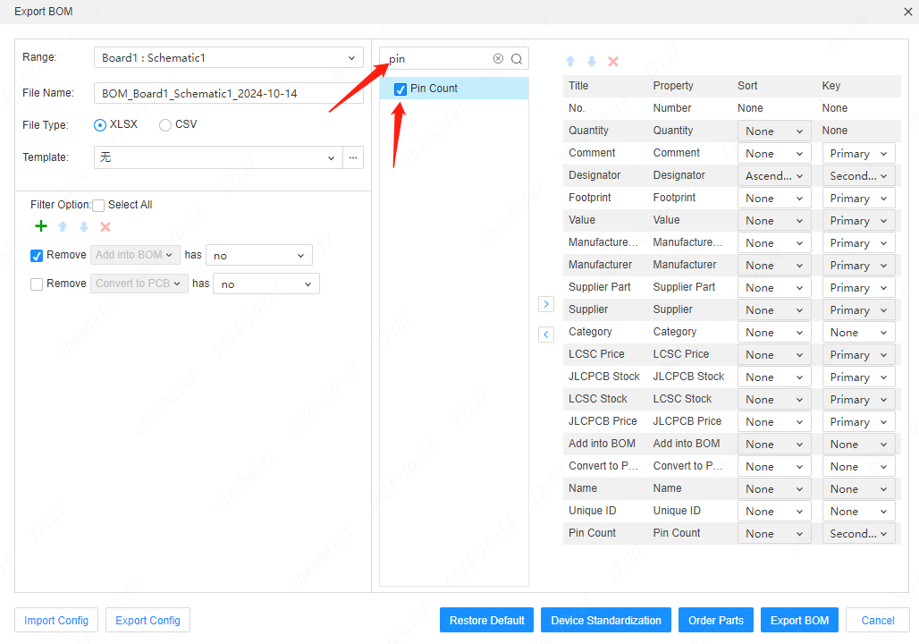
Top Menu Bar--File--Export BOM--Pin Statistics 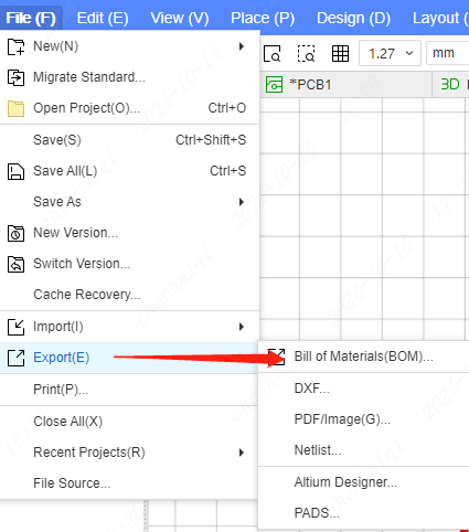
How to set the lines of a schematic diagram in the form of dashed lines, underlines, etc.?
Details
Select the line and set it in the Properties panel on the right. 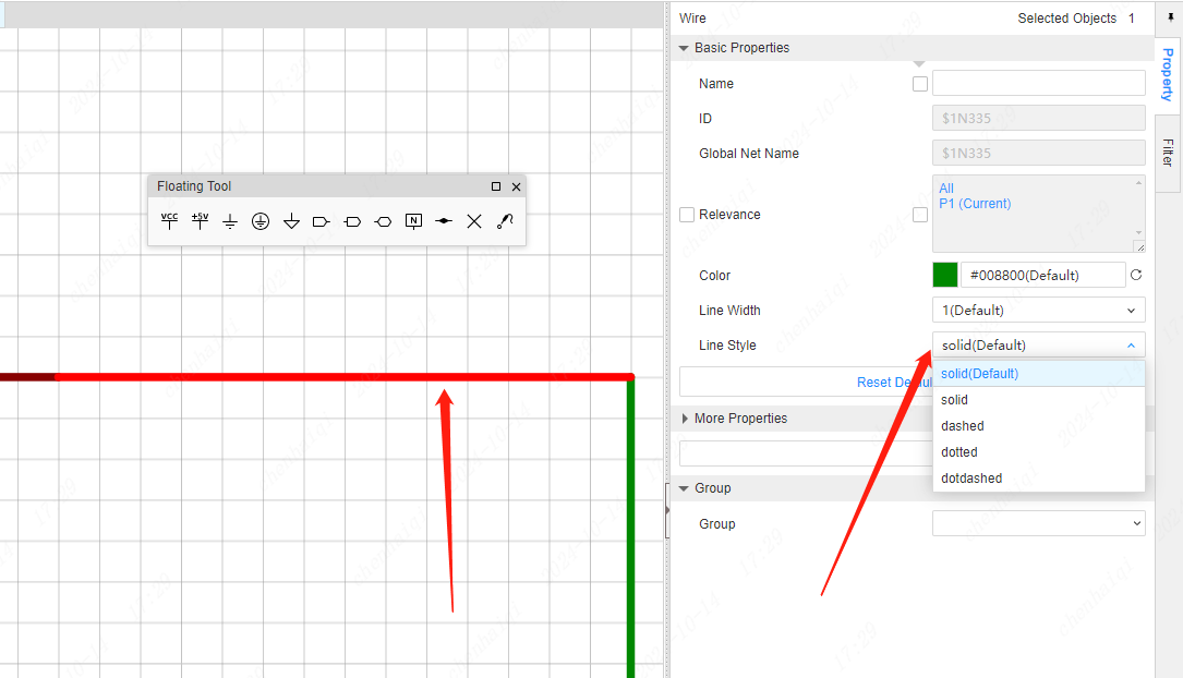
How to change the colour of the schematic Junction?
Details
The position of the colours can be modified in the top menu bar - Settings - Schematic Themes. 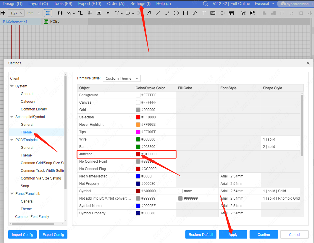
How to change the way the network is named?
Details
When the design is not given a network-specific name, the system automatically assigns network names to them as set up, and you can choose how you want to name them in the settings. 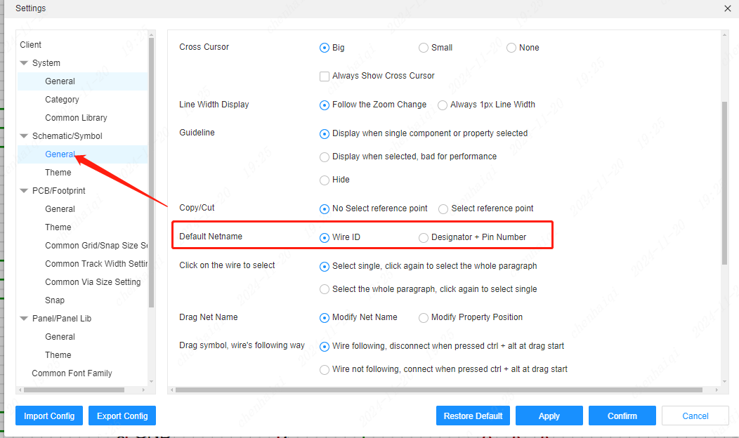


How to place the pins?
Details
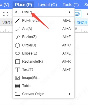
In the Pro version, the schematic does not allow direct pin placement. Because only symbols need to be configured with pins, you can add more pins to symbols in the Edit Symbol screen. 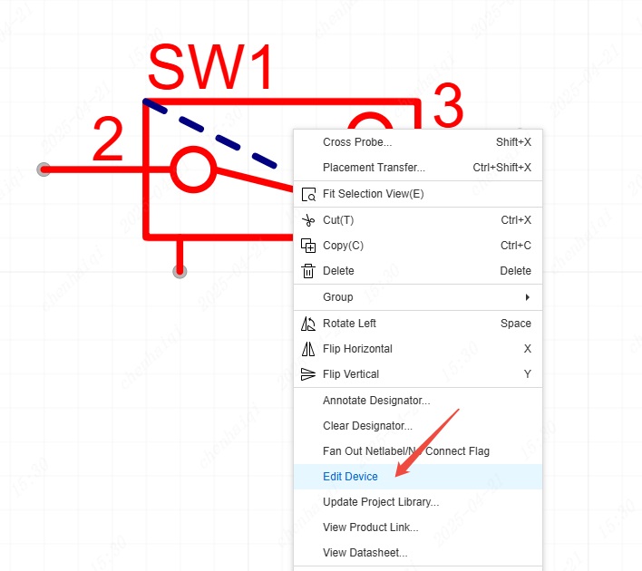
How do I fill the inside of a symbol with colour?
Details
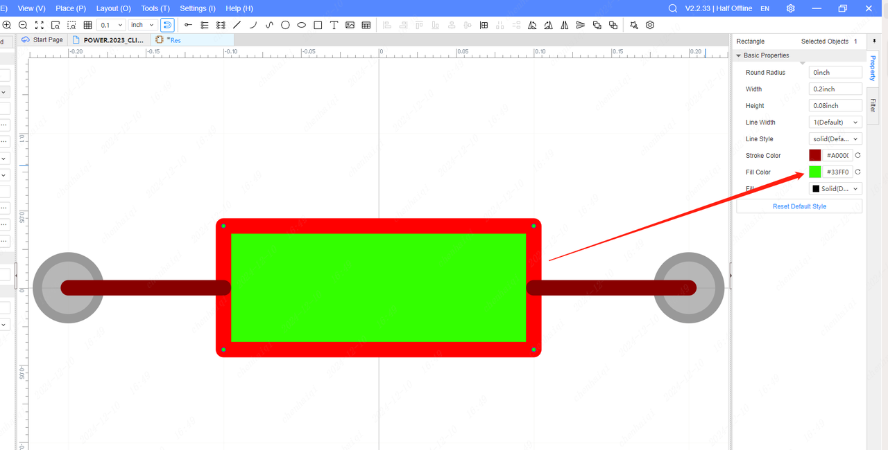
Step 1: Select the symbol you want to edit in the library and click ‘Edit device’ . 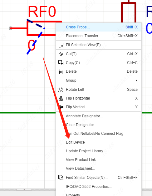 Step 2: Click on the symbol border and you will be able to choose the fill colour in the right property bar.
How to bind footprint?
Details
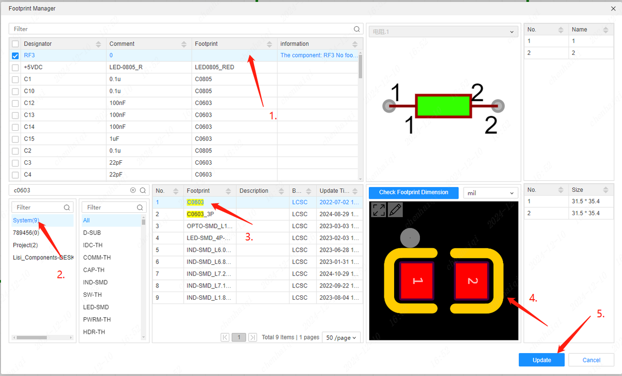
When we find that a component has no footprint, we can click on the component and click on the footprint manager in the properties bar on the right. 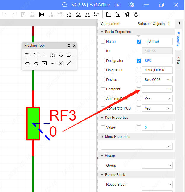 Then search for the package name you want to bind, and finally click ‘update’.
How to mirror symbols in schematic?
Details
If you want to mirror the symbols in the schematic, you can first select the symbols and then press the shortcut keys ‘X (mirror left/right), Y (mirror up/down)’. 
How to modify the error message about pad and pin mismatch?
Details
When we encounter this error, it means that the number of pads on the device's symbol pins and footprints do not match and they need to be changed to the same number. 
The symbol's pins must match the footprint's pad numbers. You can check if the device matches correctly in the footprint manager. Enter the package manager and you can see that the number of symbol pins is not consistent with the number of pads on the footprint.We can replace them with other footprints on the right side. 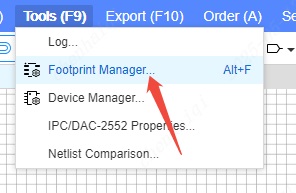
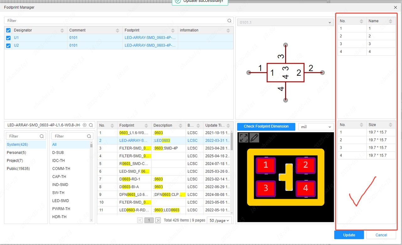
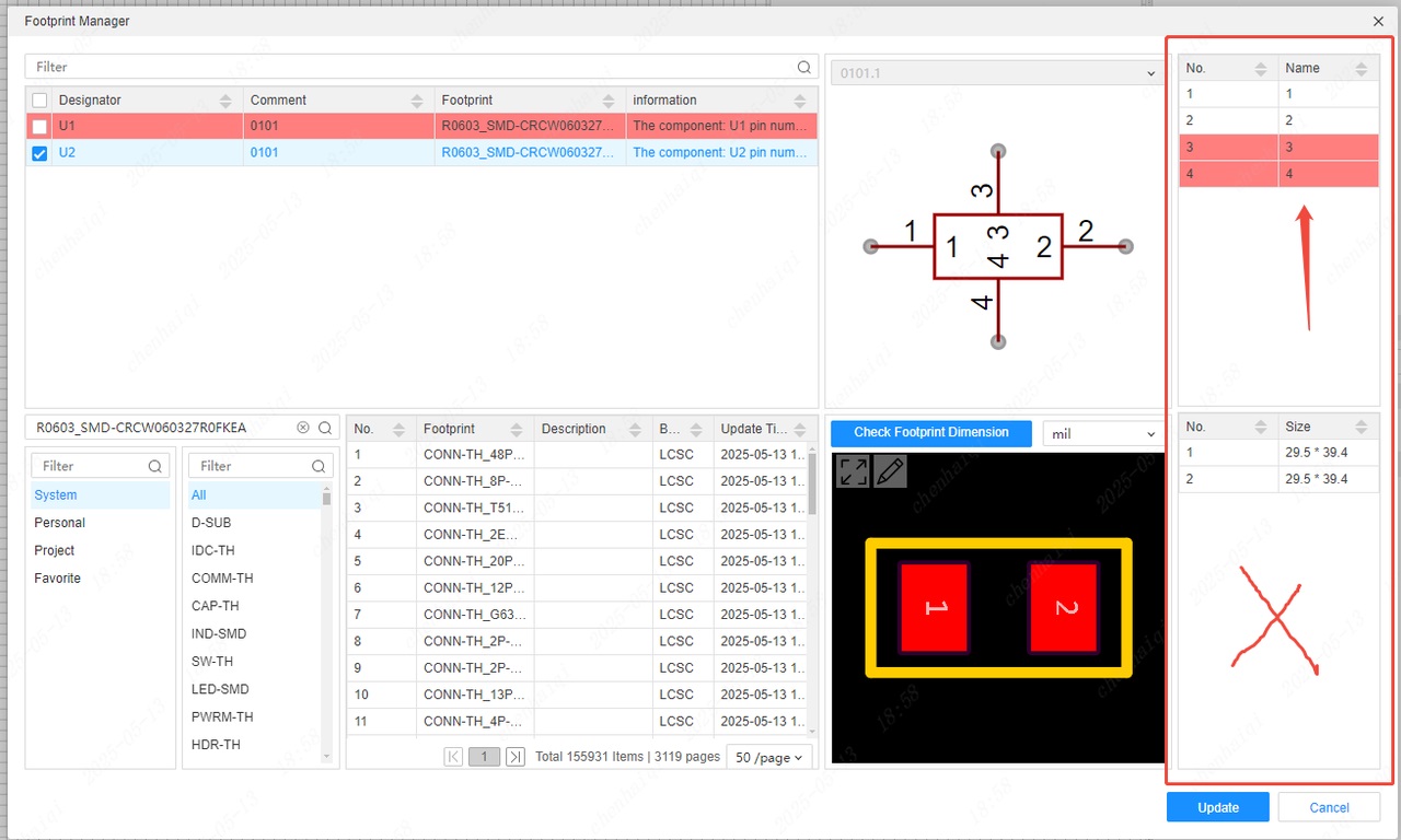 Note: The number of footprints can only be greater than or equal to the number of pins in the symbol.
What to do if a single pin error occurs?
Details
The single-pin network error means that one of your networks is only connected to one pin. 
Generally, a network name needs to be connected to two or more pins to form a connection. For example, as shown in the figure below. 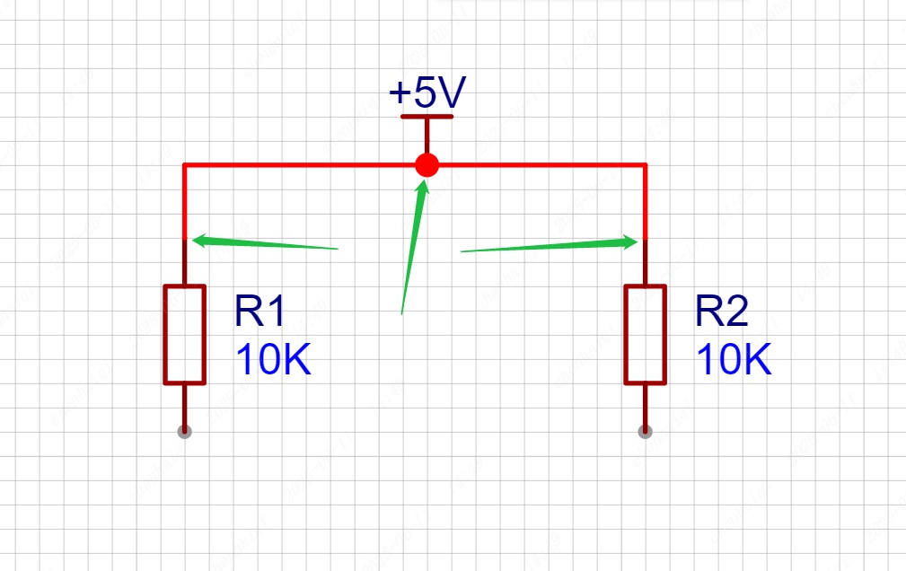
When an error occurs, it means that a network is only connected to one pin, as shown in the figure below. 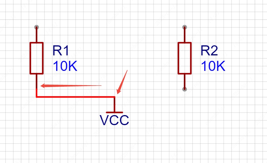
But this error is not an error that must be corrected. Because in some designs, such a single-pin design is required. It is just a reminder to tell you that you need to pay attention to this. So whether the design needs to be modified depends on the designer's own judgment. If you want to solve this error, it is very simple, just connect another pin.
How to create your own drawing template?
Details
Step 1: Find "Drawing" in the top menu bar and create a new one. 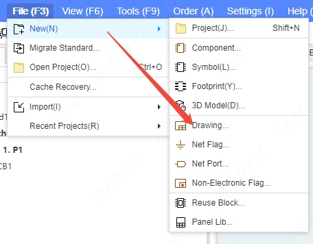
Step 2: Fill in the drawing information and properties according to your needs. Then click Save to complete the creation, and the drawing will be saved in your personal library. 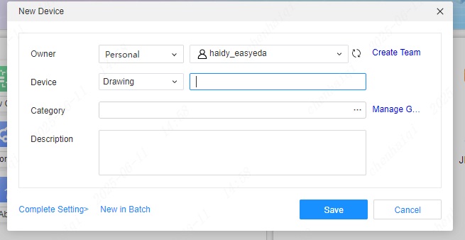
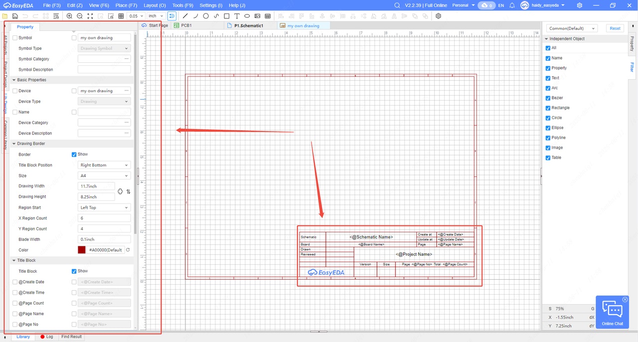
Step 3: When you want to switch the drawing panel, you can change it in the property bar on the right side of the schematic interface. 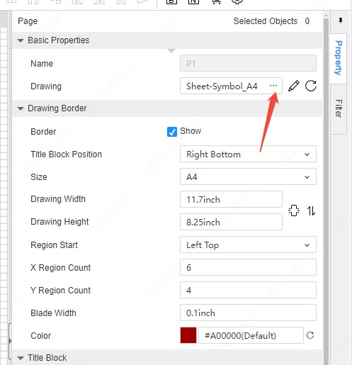
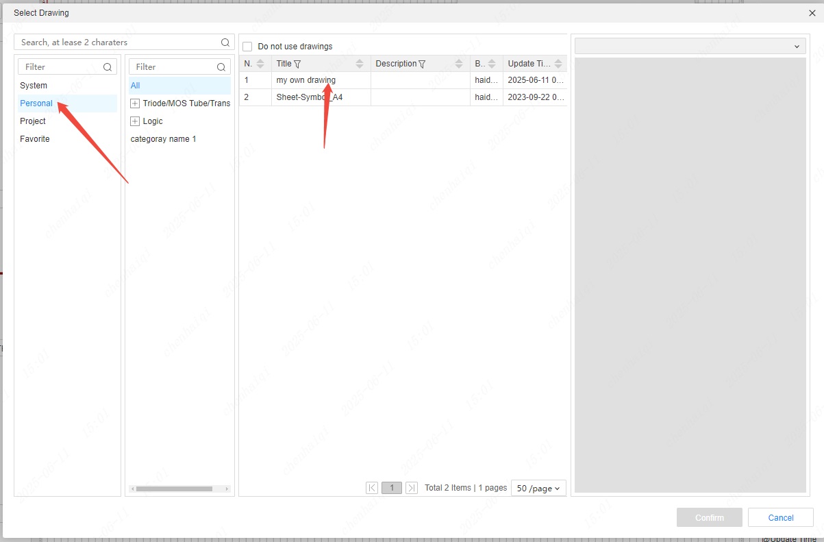
Step 4: When you want to use this template permanently, you can change it in the settings of the top menu bar. 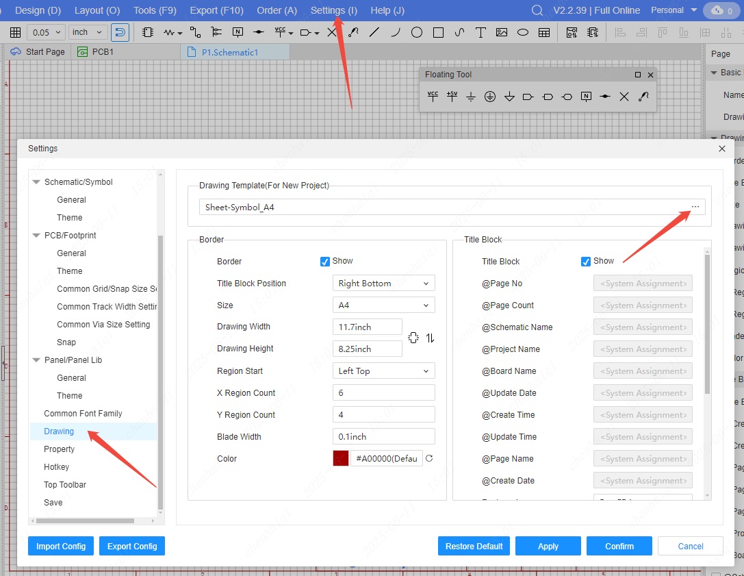
How to change the schematic drawing template?
Details
You can change the schematic drawing template. On the schematic canvas, click the Drawing button in the right-hand properties bar to access the change screen. 
We will provide some official templates for users to replace. 
You can also create your own drawing templates.Create in the top menu bar. 


Then in the same place, you can find the schematic drawing template you created in my template library. 
How do I change the pin numbering of a symbol?
Details
There are two ways to modify this. The first is to click the symbol pin and change the pin number in the properties bar on the right. However, this method does not support changing the pin name. 
The second method is to select the symbol and right-click to enter the symbol editing interface. Then click the symbol pin and modify the pin number and pin name in the property bar on the right.However, please note that the pin number and pin name of the symbol must be consistent with the pad number and pad name of the footprint. 

How to place multiple components?
Details
In EDA, there are multi-component devices. A multi-component device is a device that has two or more symbols but only one footprint. Furthermore, the Designators for multi-component device symbols in EDA is as follows: for example, (U1.1, U1.2...), (R2.1, R2.2, R2.3...). Therefore, you should also pay attention to this issue when you need to create multi-component devices or modify device Designators. When placing components, it's important to click continuously; you can't place a component, cancel, and then re-place it. 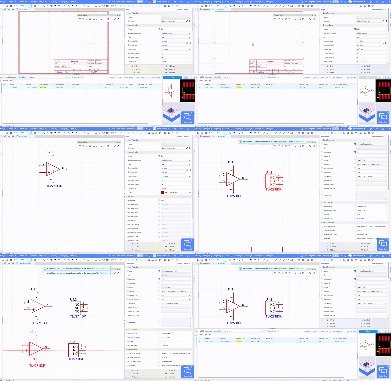
How can I import a DXF file into EasyEDA and use it as an element?
Details
Both schematics and PCBs can import DXF files as line elements. The function to import DXF files can be selected in the top menu bar of the schematic diagram. 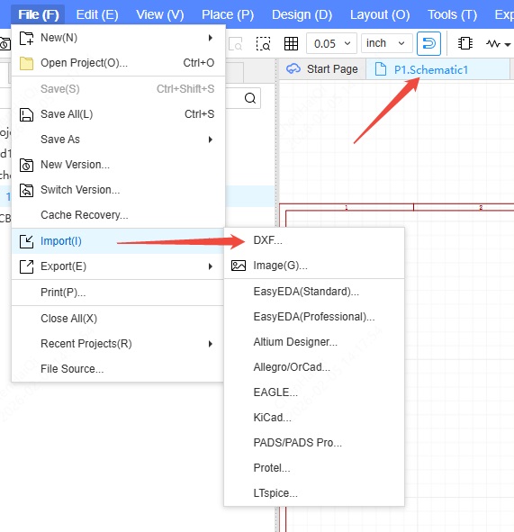
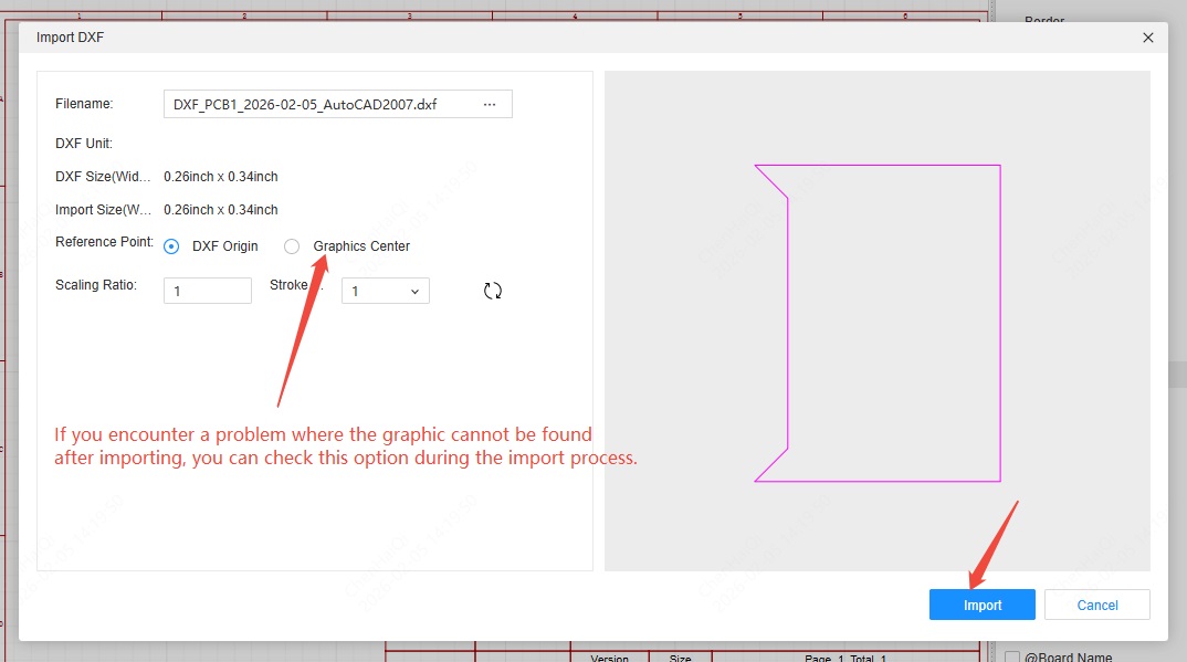
After importing, select the imported lines, and you can modify some attribute information in the properties panel on the right. 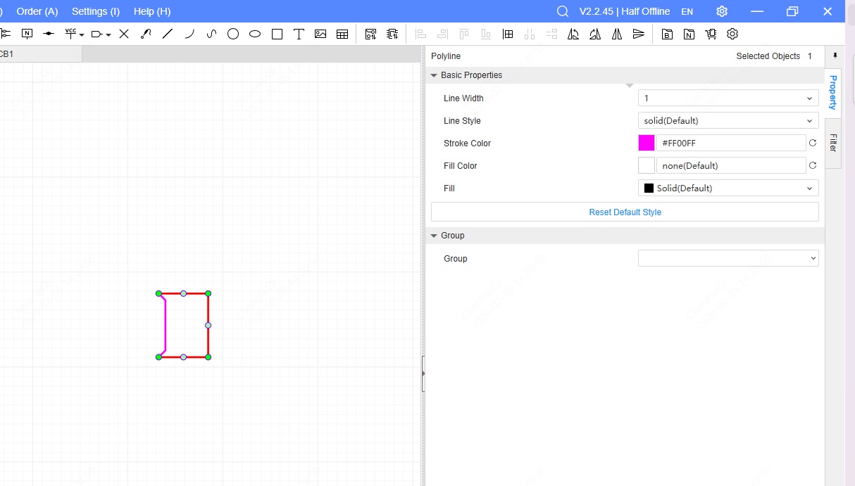
You can import files in the same way in a PCB. 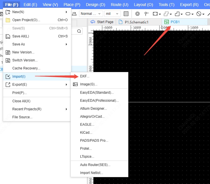
In the import interface, you can choose which layer you want to place these lines on. 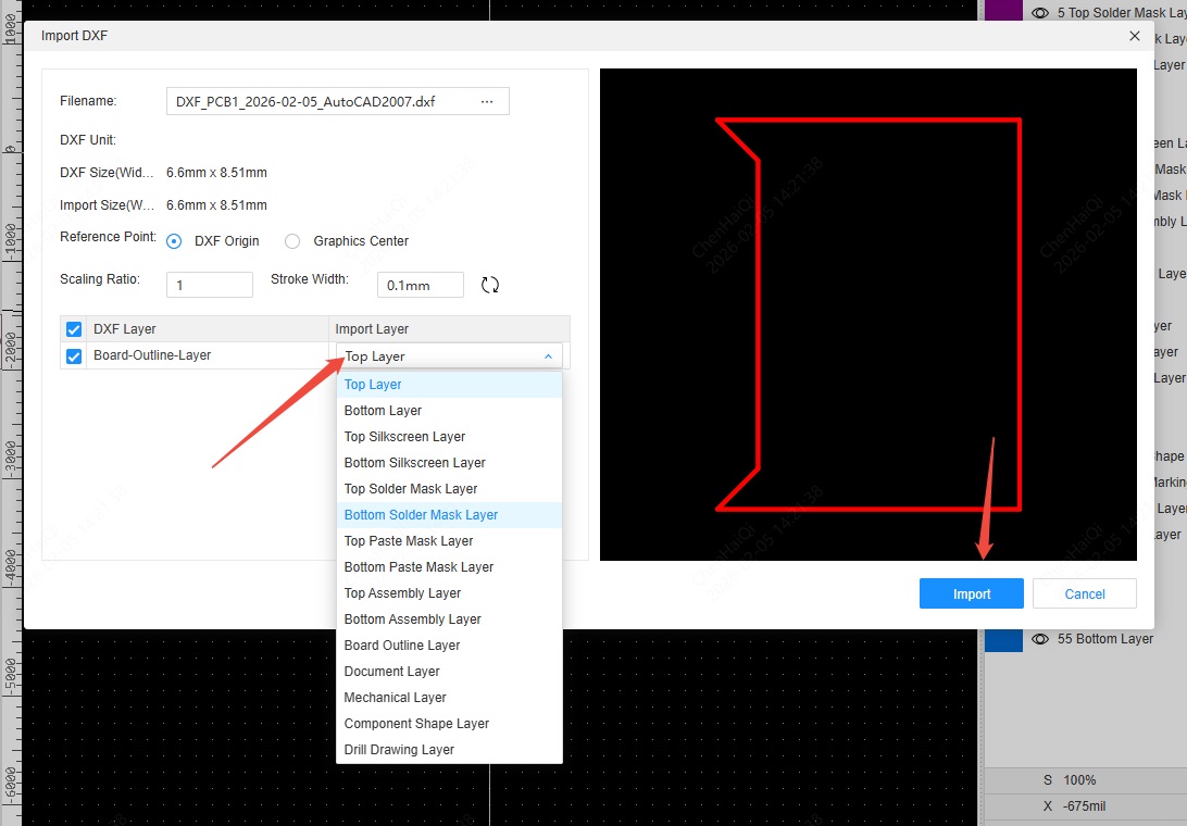
You can also select the line and modify its properties in the right-hand properties panel after placing the DXF file. Alternatively, you can select the line, right-click, and choose "Convert to Other Elements". 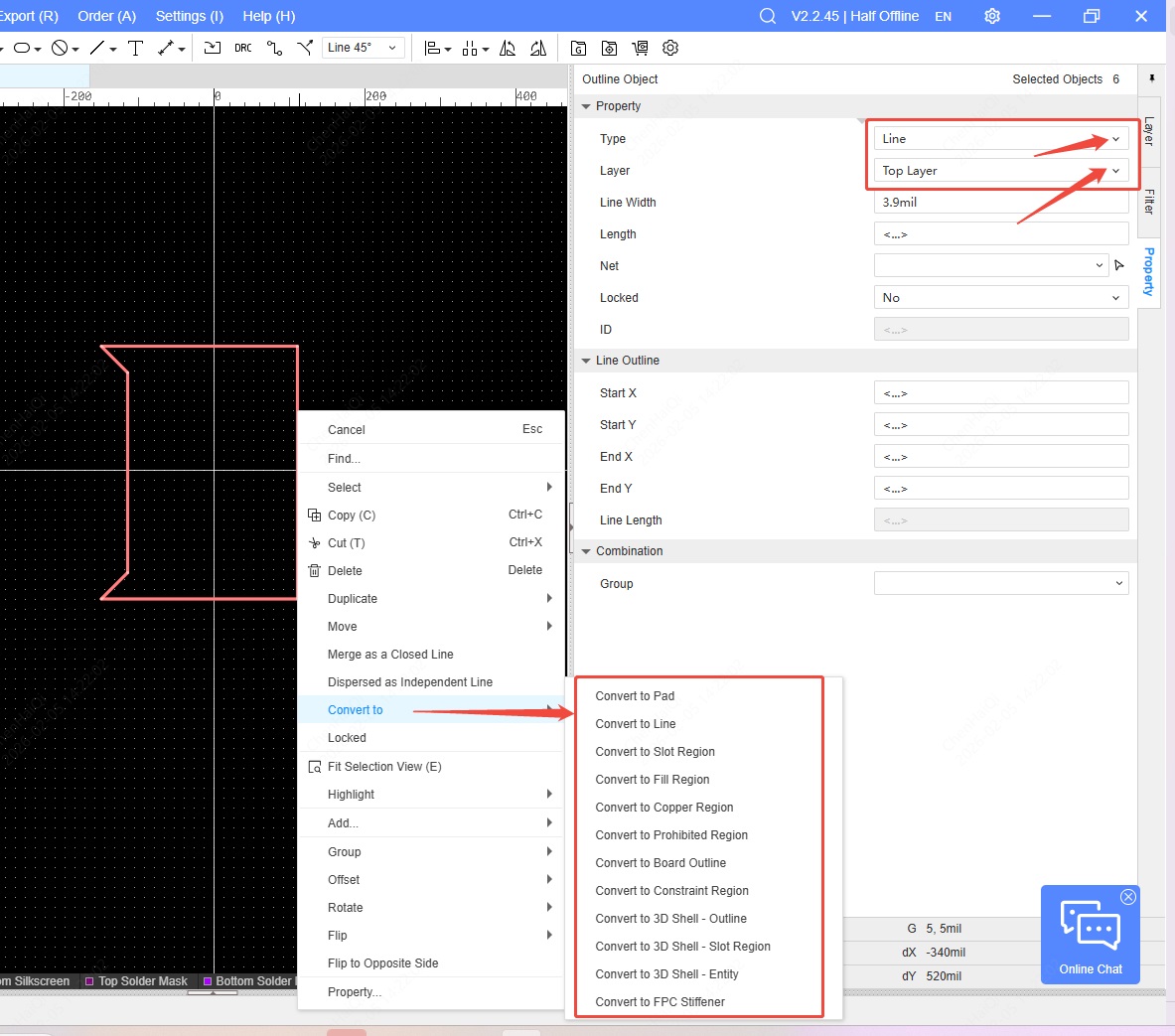
This allows you to import DXF files and transform them into board outlines, silkscreens, copper pours, and other elements. You can also place them on different layers.
How to export a custom PDF file?
Details
Both schematics and PCB layouts can be exported as PDF files, and both can be exported as custom files. In the schematic interface, you can find the export function in the top menu bar. 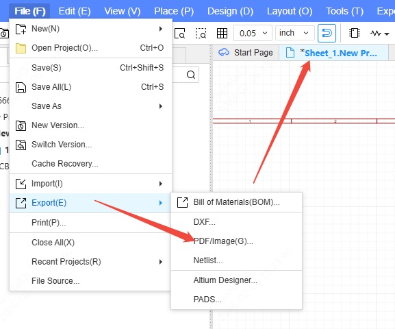
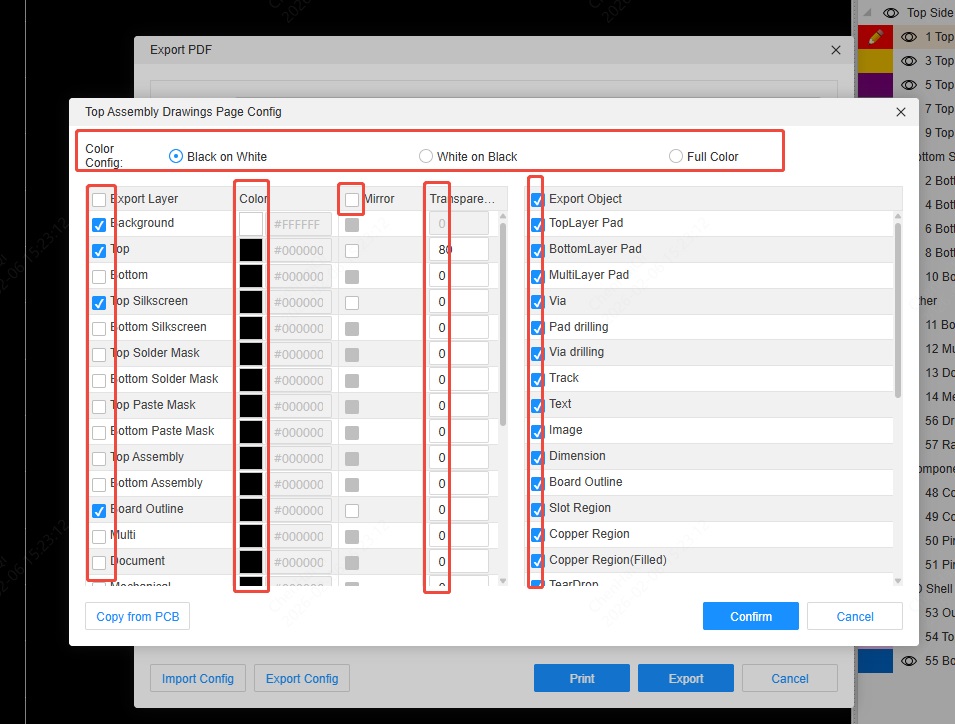
In the export panel, you can see some custom options, which you can choose according to your needs. You can choose basic settings such as File Type, Theme, Line Width, and Size. There are also special watermark settings that can be added. You can also choose to export a PDF file of a specified schematic or drawing page. 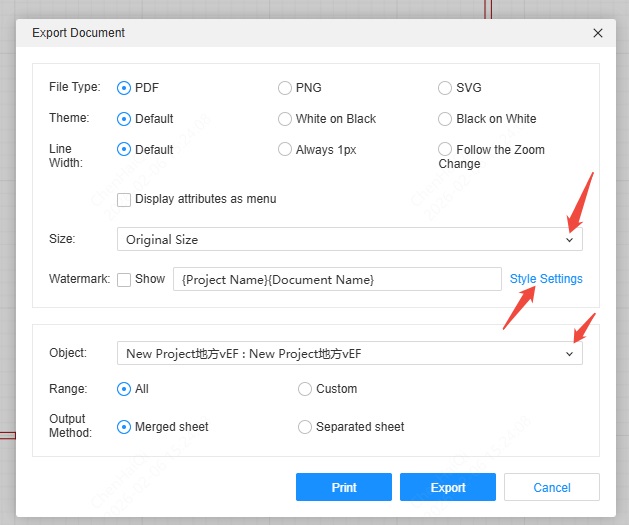
The same applies to the PCB interface. 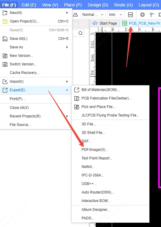
PCBs also have the same basic settings as schematic diagrams. 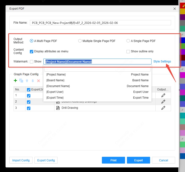
But most importantly, the PCB supports customizing the settings for each layer. Clicking "Edit" will take you to the settings interface for each page. You can select the layers and elements to export, as well as adjust their colors and transparency.
After setting all the configurations, you can export the PDF file you want. 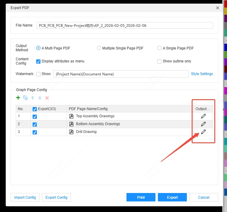
How to rotate a schematic and resize imported images?
Details
Step 1: Import the image. 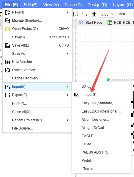
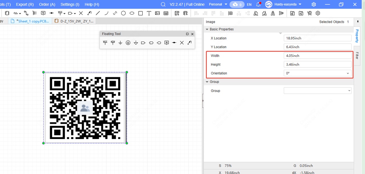
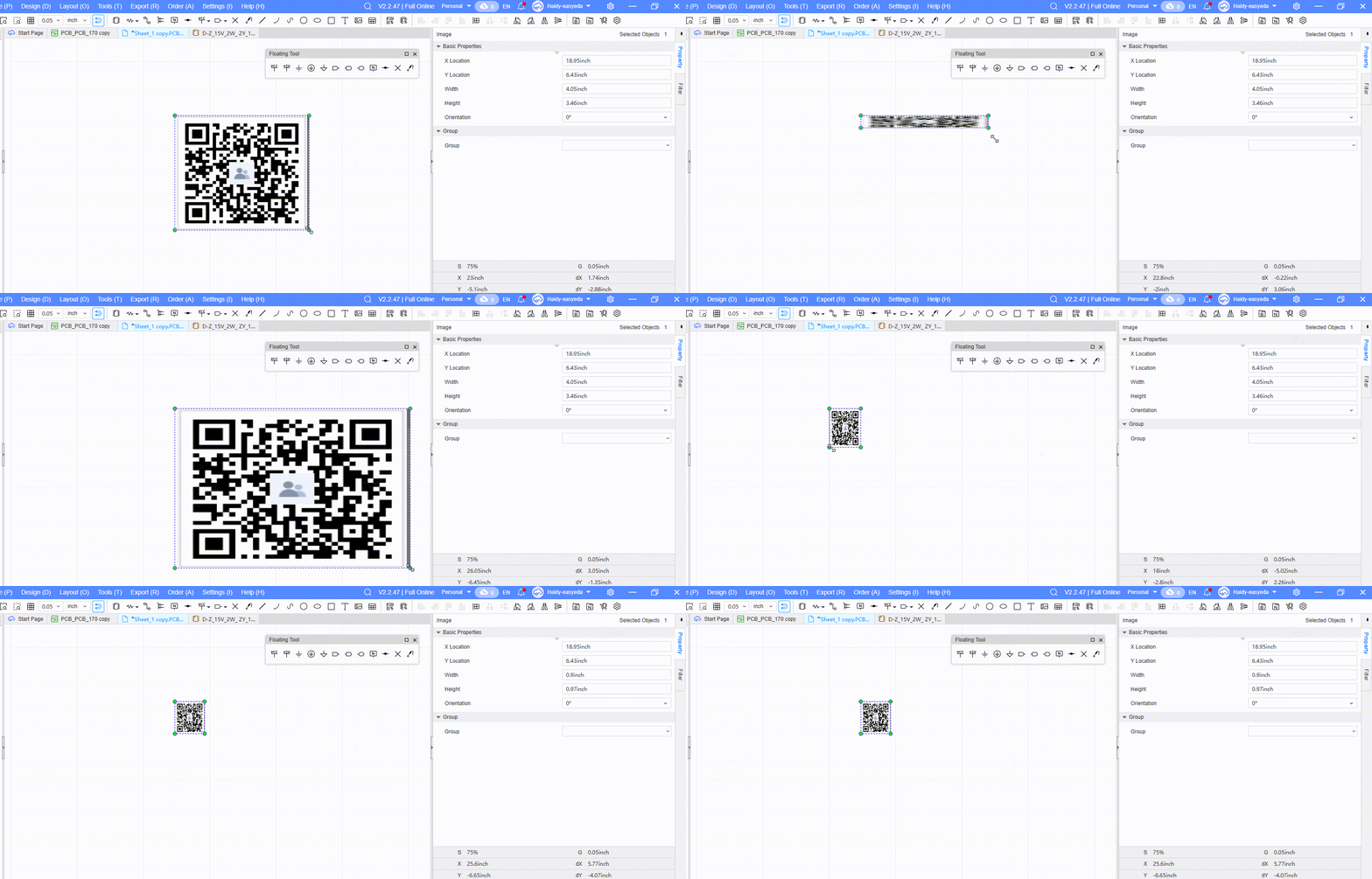
Step 2: Select the image and choose the rotation angle in the properties panel on the right.You can also modify the height and width. 