Snap
EasyEDA Pro provides users with powerful adsorption function, which supports adsorption to certain specific positions of existing elements on the canvas during wiring, measurement, drawing and other operations, making it convenient for users to quickly align and accelerate design efficiency. At the same time, the range and position of adsorption support can be customized by users, which can adapt to different user habits
Instructions:
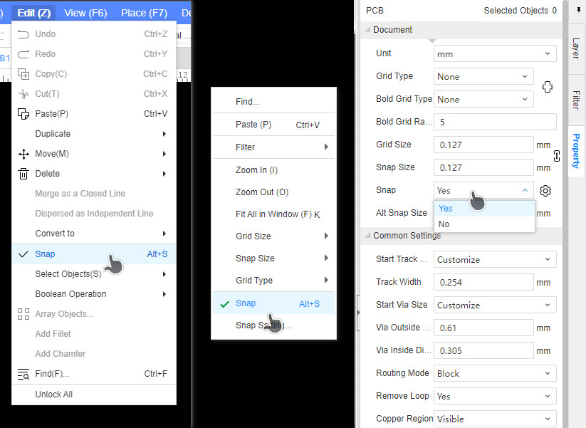
- Top menu - Edit - Snap
- Right-click - Snap
- PCB right-side panel - Snap
- Default shortcut key Alt + S
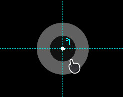
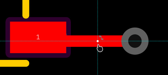
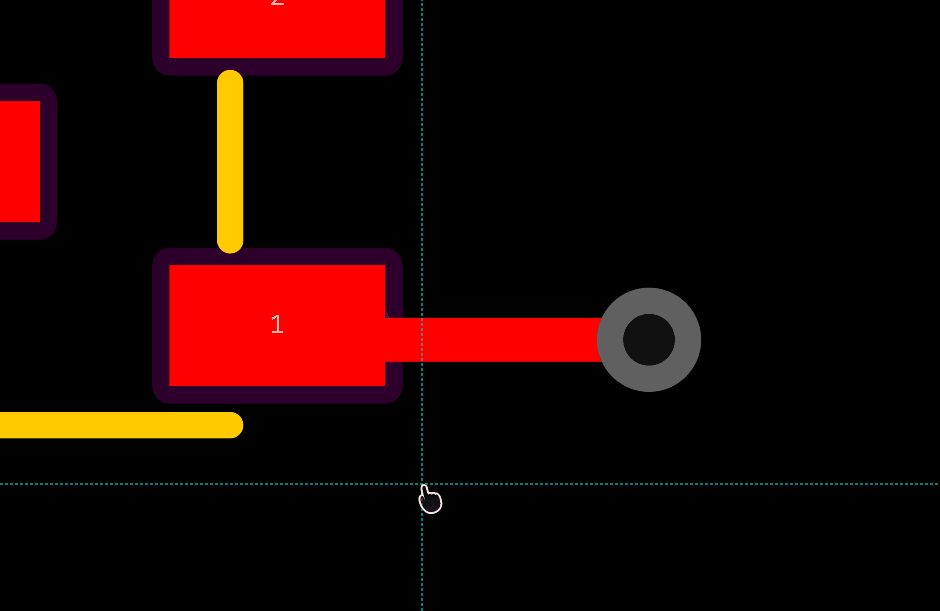
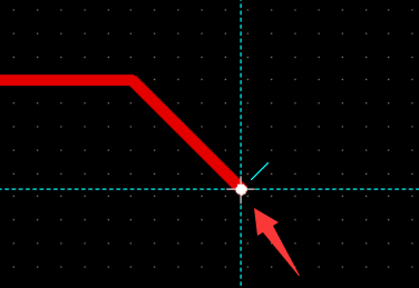
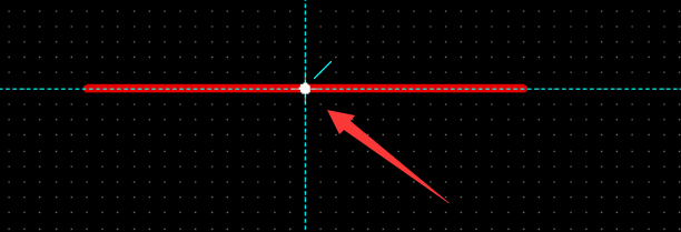
After opening the adsorption, move the mouse to the adsorption range, and it will automatically adsorb, and a white dot will be displayed at the adsorption position
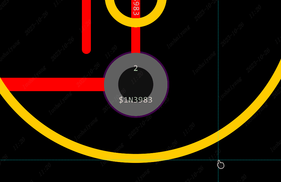
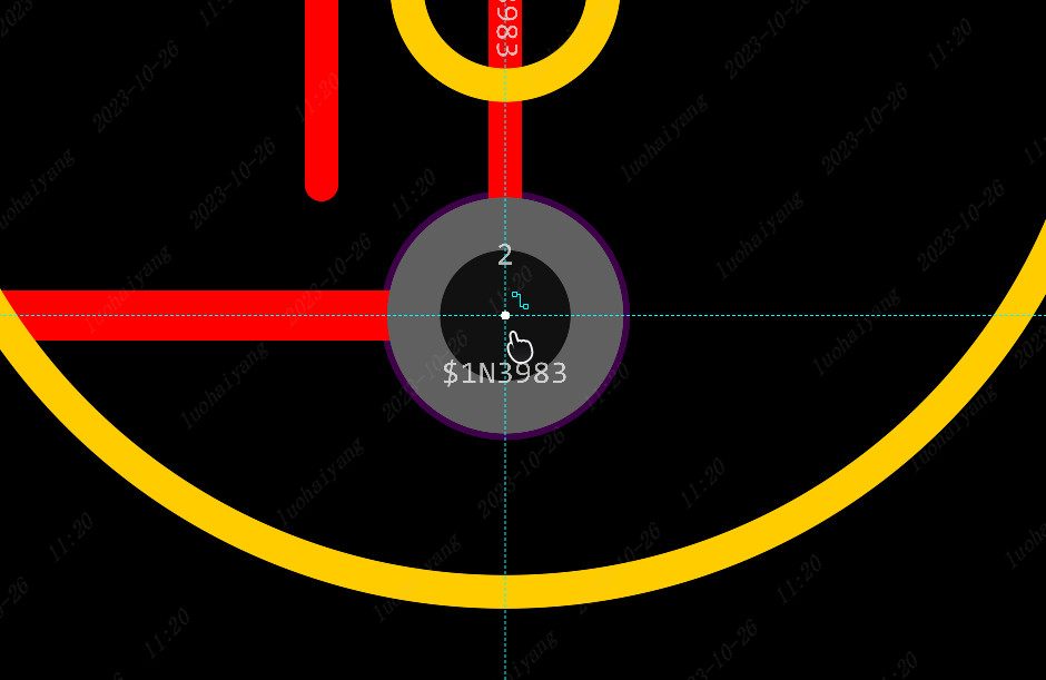
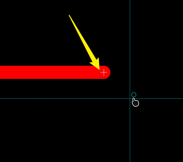
When performing some operations other than drawing wires, if some positions on the canvas are adsorbed, a white cross adsorption mark will also be generated, up to six of which can exist on the canvas at the same time. This mark can be used for operations such as extending the line adsorption. Scaling the canvas or exiting the current operation will clear all marks
Adsorption setting
We can configure the desired adsorption distance and adsorption position in the adsorption settings.
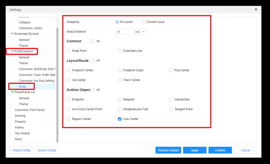
Adsorption layer configuration
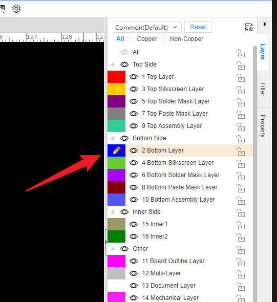
It can be set to adsorb all layers or only the current active layer . When it is set to only the current active layer (where the pencil icon is is the current active layer), it will not adsorb the positions on the elements of other layers. Selecting all layers is the opposite. Wiring is not affected by this configuration , only the current active layer will be adsorbed
Adsorption distance
The adsorption distance can be set at this position. Note: During wiring, adsorption will only begin in the pad or via. Therefore, even if the mouse is already within the adsorption range during wiring, if it is not inside the above graphic element, it will not produce adsorption effect.
General purpose
In all the check boxes on the right side, you can check or uncheck the grid points and extension lines at the same time, the same below
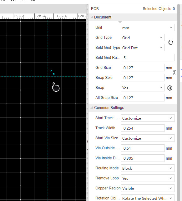
Grid points
After checking, the cursor will be attached to the grid points on the canvas, and the white points will not be displayed when attached to the grid
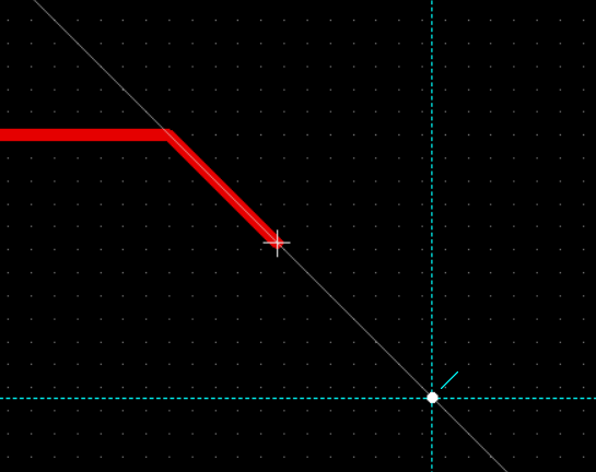
Extension cord
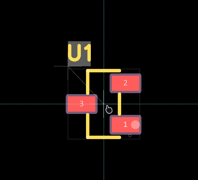
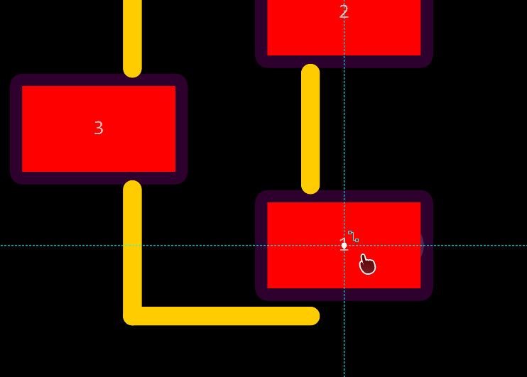
When drawing lines, using the movement function to move elements, adjusting the outline object shape and other operations. Some cross adsorption marks will be generated. When moving the mouse to the direction of the line extension or orthogonal position, it can be adsorbed on the extension line for easy alignment
Layout wiring
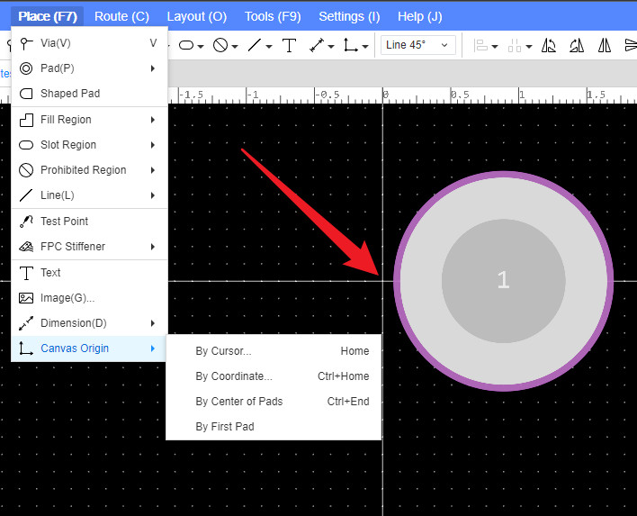
Encapsulation origin
After checking, it can be adsorbed to the origin of the package. The origin of the package is the center position of the cross in the package, which can be modified by placing the menu when drawing the package
Packaging center
After checking, it can be attached to the center point of the entire encapsulation graphic. Only one of the encapsulation center and encapsulation origin options can be selected at the same time
Center of solder pad
Check the center point of the pad pattern that can be adsorbed
Center of via
Check the center point that can adsorb through the hole
Center of conductor
After checking, it can be adsorbed to the wire
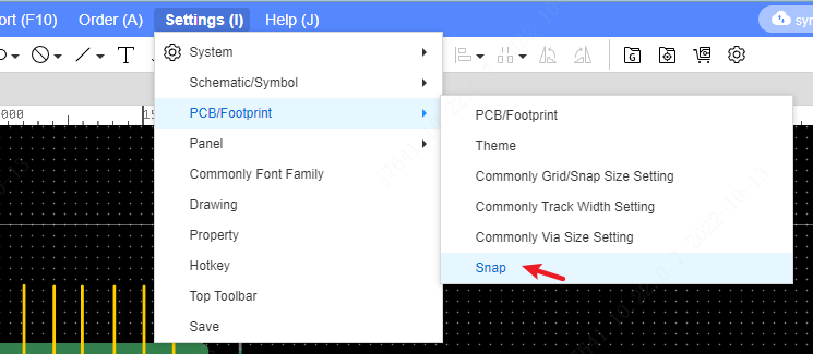
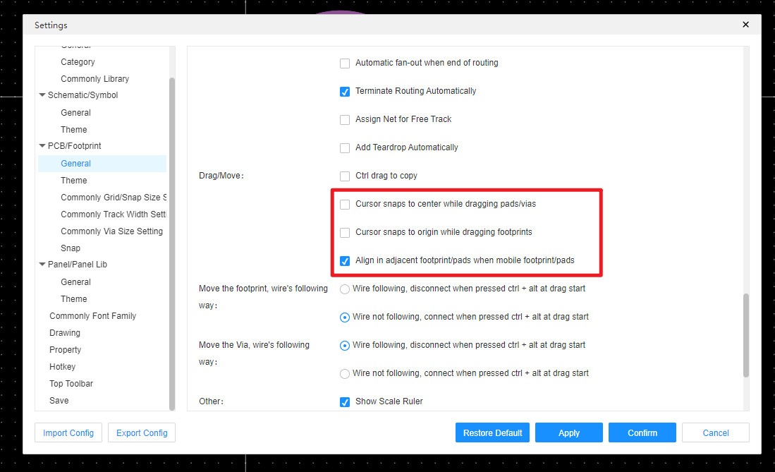
Entrance: Top Menu - Settings - System Settings - Snap
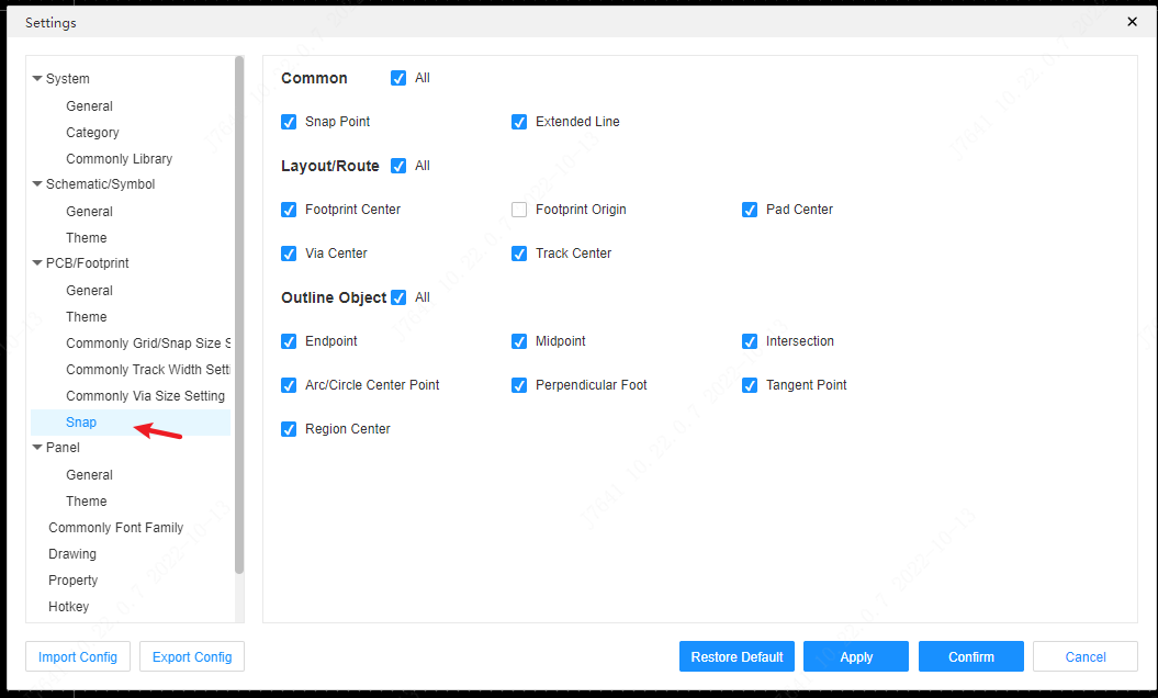
Outline object
Endpoint
The endpoint at the end of the polyline, this setting is only valid for polylines.
Midpoint
After checking, it can be attached to the center point of the line segment of the line or contour object.
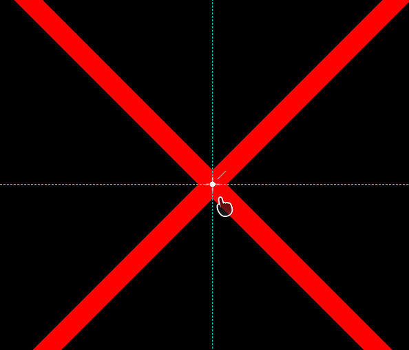
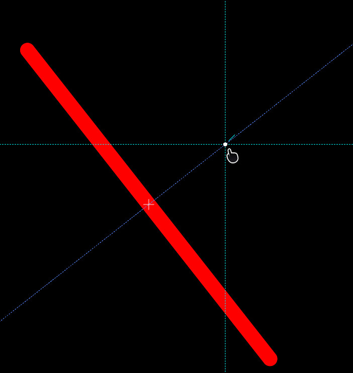
Intersection point
After checking, you can adsorb the intersection points between two or more lines in the same layer.
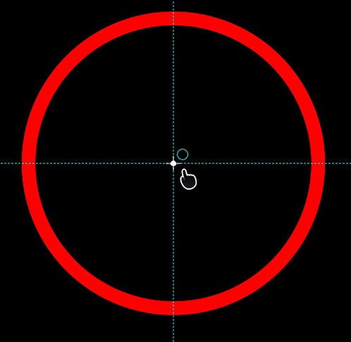
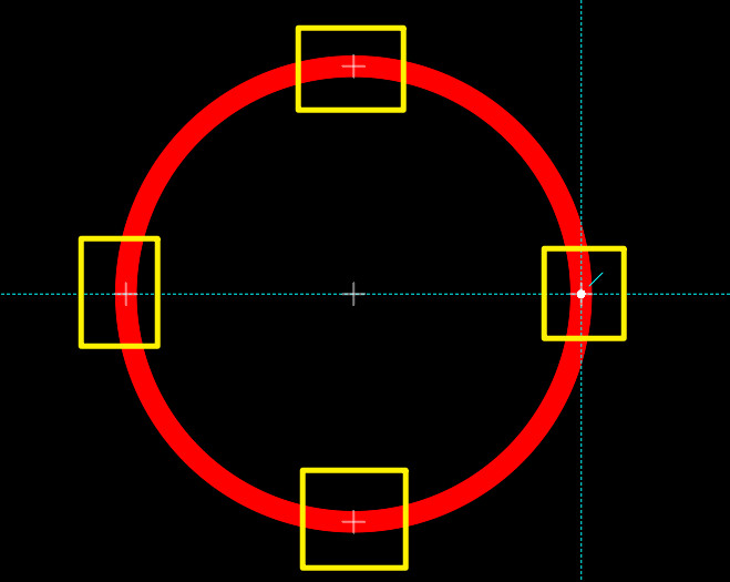
Center of circle
After checking, the center points of circles and arcs can be adsorbed. You need to move the mouse to the prototype's ring before the middle adsorption mark will be generated
Vertical foot
After opening this item, you can adsorb to the vertical line based on the line segment that produces the adsorption mark
Tangent point
After this option is selected, it can be attached to four tangent points of the prototype orthogonal tangent
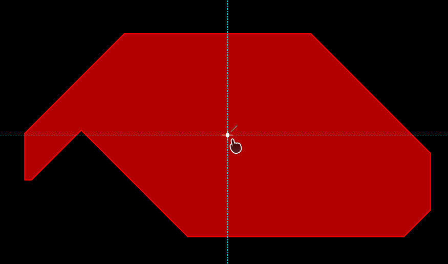
Regional centres
After checking, it can be adsorbed to the graphic center point of contour objects such as copper paving area and filling area.
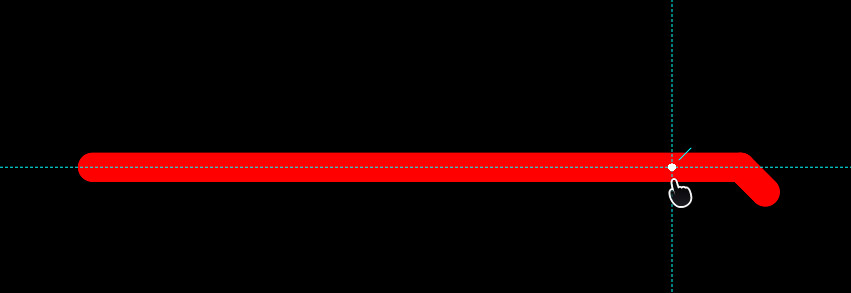
Center of line segment
After this option is selected, it can be adsorbed to the center of the line segment, similar to the adsorption of the wire center
Other adsorption
In PCB conventional settings, some adsorption effects can be opened when dragging packages or solder pads