Update PCB/Convert Schematic to PCB
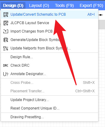
When you have finished drawing the schematic and want to convert it to PCB, you can click Top Menu > Design > Schematic to PCB
Notice:
- To update from schematic to PCB, both schematic and PCB must be under the same board.
When the schematic diagram is transferred to the PCB, it will be checked first according to the design rules of the schematic diagram, and then converted after meeting the conditions for transferring to the PCB.
Check footprint
After clicking "Schematic to PCB", if the editor detects that the corresponding information of components and footprints is abnormal, an error dialog box will pop up, and the conversion will not continue. You need to fix errors in the footprint manager. Because EasyEDA Pro will record the unique ID of the footprint in the symbol library and schematic diagram when specifying the footprint, so the error message corresponds to the following:
- There is a specified footprint name, but the specified footprint library title has been modified by the creator
- There is a footprint name, but no footprint has been specified through the footprint manager
- The symbol library pin number name is inconsistent with the specified footprint pad number name
- The number of symbol library pin numbers is greater than the specified number of footprint pads
- footprint is empty unspecified footprint
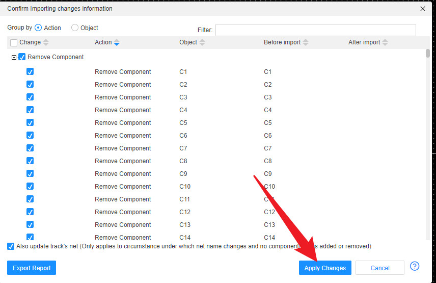
Confirm the introduction information
If there is no problem with the schematic diagram, it is successfully imported to PCB. The pop -up window as shown in the figure below will appear.
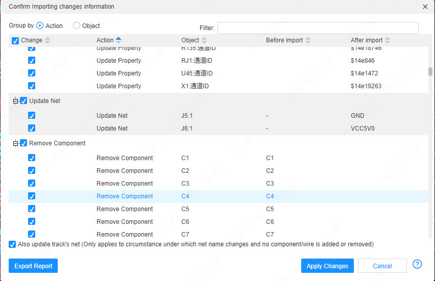
Select all the changes in the default in the pop -up window. If you don't need some changes, you can cancel the check on the left
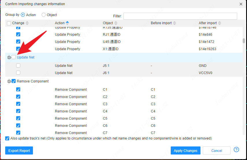
You can also set different grouping and sorting, as well as filtering the content
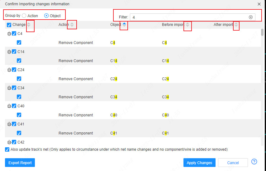
You can also export the content displayed in this window into a table
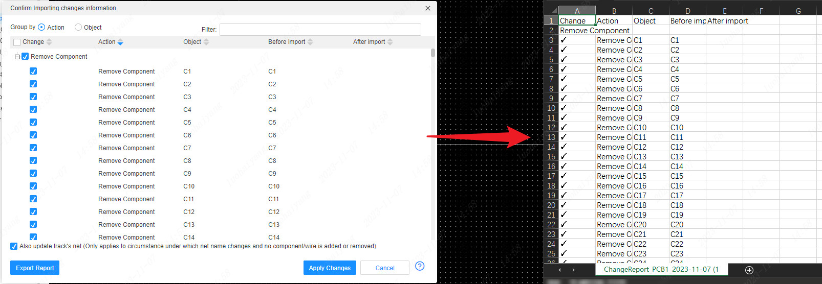
Click the application to modify it to modify the check content to the PCB
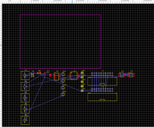
Generate PCB
After the conversion is successful, as shown in the figure below, the PCB footprints are automatically arranged in a row in order. The blue flying wires indicate that the two pads need to be wired and connected, which belong to the same network.
Update PCB
When you have completed the transfer PCB action, but modified the schematic again, you do not need to transfer a new PCB, just click "Update PCB" to update the changes to the existing saved PCB file.
Changes can also be imported directly in the PCB: Top Menu - Design - Import Modification Information.
Because the schematic net name is generated after calculation, if some nets are changed after you modify the schematic, after updating to the PCB, the routed layout of the original net will remain unchanged.
Update the pad network and update the wires related to the pads with the pad network update. There may be changes in the wire network. You need to manually change the old network name of the wire to the new network name!
Most schematics can be updated to the PCB after updating the net. However, if the schematic diagram has added or deleted devices, the wire network of the PCB needs to be manually modified.