Copper Region
If you want to keep the entire copper area for grounding or power, you can use the "Copper" function.
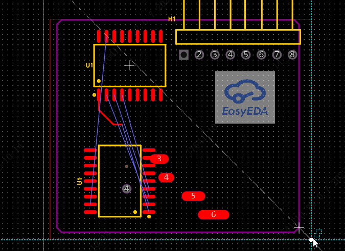
After clicking, you can draw the copper area around the area you want to copper. You can draw directly outside the board border, and you don't need to follow the board border. EasyEDA Pro will automatically cut the excess copper foil.
The top and bottom layers need to be drawn separately. A board can draw multiple copper areas and set them separately.
- Top Menu - Place - Copper Region - Rectangle (choose according to personal needs)
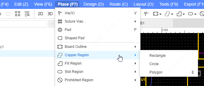
Draw rectangular copper skin
After drawing, the net that is connected to the copper region will be automatically set up,You can modify the layers, networks and other attributes of the copper area through pop -up windows.
Priority automatic adjustment
After drawing a copper paving, a copper paving is completely included in another copper paving of the same layer, which will automatically increase the priority of the internal copper paving, so that the internal paving can be paved out, and these copper is automatically reconstructed.
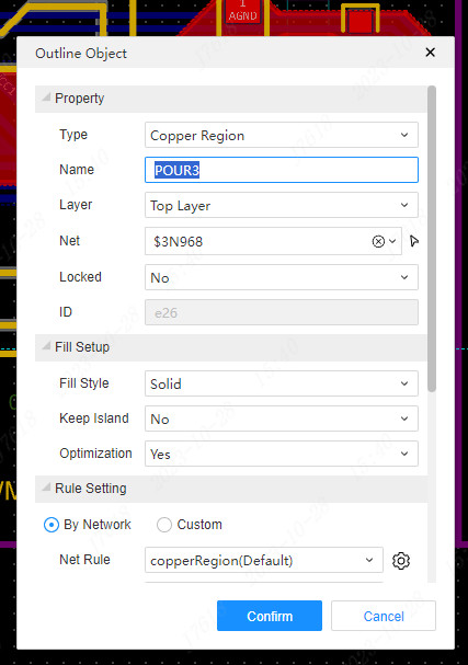
Copper Property
Type: Outlie object defaults to copper region type;
Name: Different names can be set for the copper region.
Layer: The layer of the copper area can be modified: top layer. bottom layer. inner layer 1. inner layer 2. inner layer 3. inner layer 4. When the type of the inner layer is the inner electric layer, the copper layer cannot be drawn;
Net: Set the network the copper foil is connected to. When the network is the same as the element network on the canvas, the copper can be connected to the element and it will be displayed, otherwise the copper will be considered as an island and be removed.
Locked: Only lock the position of the copper. After locking, the size and position of copper laying cannot be modified through the canvas;
Fill Style: Full Fill: Normal copper fill style; 45 degree net: The area is filled with a 45 degree grid fill. 90 degree net: The copper fill in this area is a 90 degree net type.
Keep islands: yes or no. That is, whether to remove dead copper. If there is no network set for copper region, then the entire copper region will be regarded as dead copper and removed. If you want to keep the copper region, you can choose to keep the island or set up an existing network on the PCB for the copper region, and rebuild the copper region;
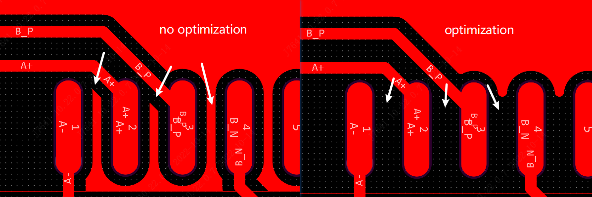
Optimization: Appears only when the fill style is full fill, and the mesh copper region enables manufacturing optimization by default. The default is yes, the sharp corners and thin copper wires less than 8mil will be removed, which is convenient for production; set to otherwise, the sharp corners and thin copper wires will be displayed;
Rebuild copper region:Rebuild according to the selected copper.The shortcut key Shift+B will rebuild all copper (including the internal electrical layer).
Place/remove suture via:Automatically placed suture holes (batch holes) according to the selected copper.
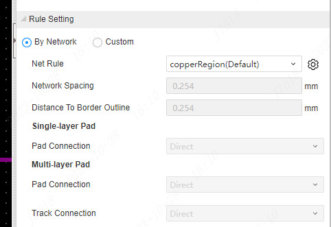
Rule setting:You can switch the copper paving rules and custom copper paving rules according to the network.It does not support the attributes of copper paving directly.
Right -click menu
The right -click menu after selecting the copper area provides a lot of fast functions.
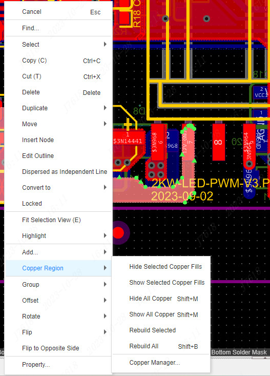
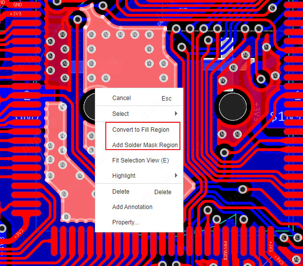
- Edit contour: Modify the outline shape of the copper.
- Turn to: Turn the copper -paving area to a fill area, prohibit the area, etc.
- Bald copper area: can display hidden copper -paving areas; rebuilding copper -paving areas.
Hidden display copper
EasyEDA supports a variety of functional entrances to hidden copper paving.
- Click the copper right -click menu or the top view menu for hidden display
- Click on the right attribute panel on the right side of the canvas blank, hide the copper area
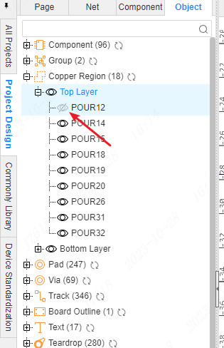
- Click on the left object tree, click the copper -paved eye icon to hide
- Click on the right filter panel and click the copper -paved eye icon to hide
Select Copper
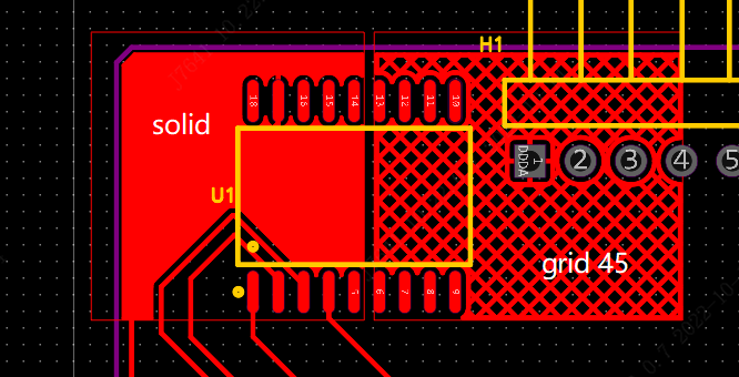
In the PCB theme settings, the copper region can set different border line types.
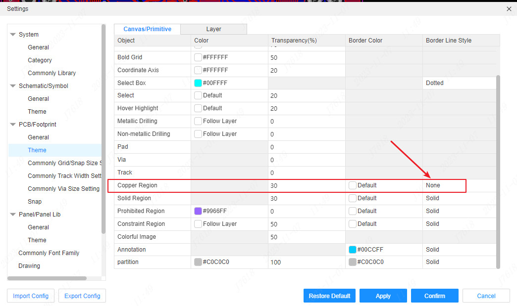
When the border line style is set to solid or dotted, the copper frame is fixed as a solid or dotted.
When the border line type is set to the same time, the copper -paving area of the copper will automatically hide the border, and the copper -paving area that is not paved still displays the frame.
After the copper is paved, click the copper filling position, and the copper paving area where the copper is filled will be automatically selected. If the frame is hidden, it will be automatically displayed at this time.Live CTRL and select multiple borders for Burrough operation.
Click the copper filling position again to switch to the chopped copper filling. At this time, if you press and hold the CTRL to click to select other copper filling positions, you can choose more filling.Wait for operation.