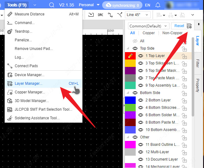
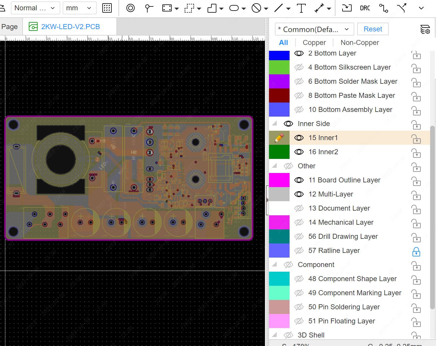
Layer Manager
EasyEDA Pro edition provides users with a layer manager, users can quickly configure PCB layer related content in the layer manager, such as the number of PCB layers, layer color, type, transparency and so on
Steps:
- Top Menu - Tools - Layer Manager
- Click the layer manager icon in the upper right of the layer property bar on the right
The layer manager window pops up, where you can set the transparency, name, type, and add layers of the layer.

add layer
Select the number of layers to add
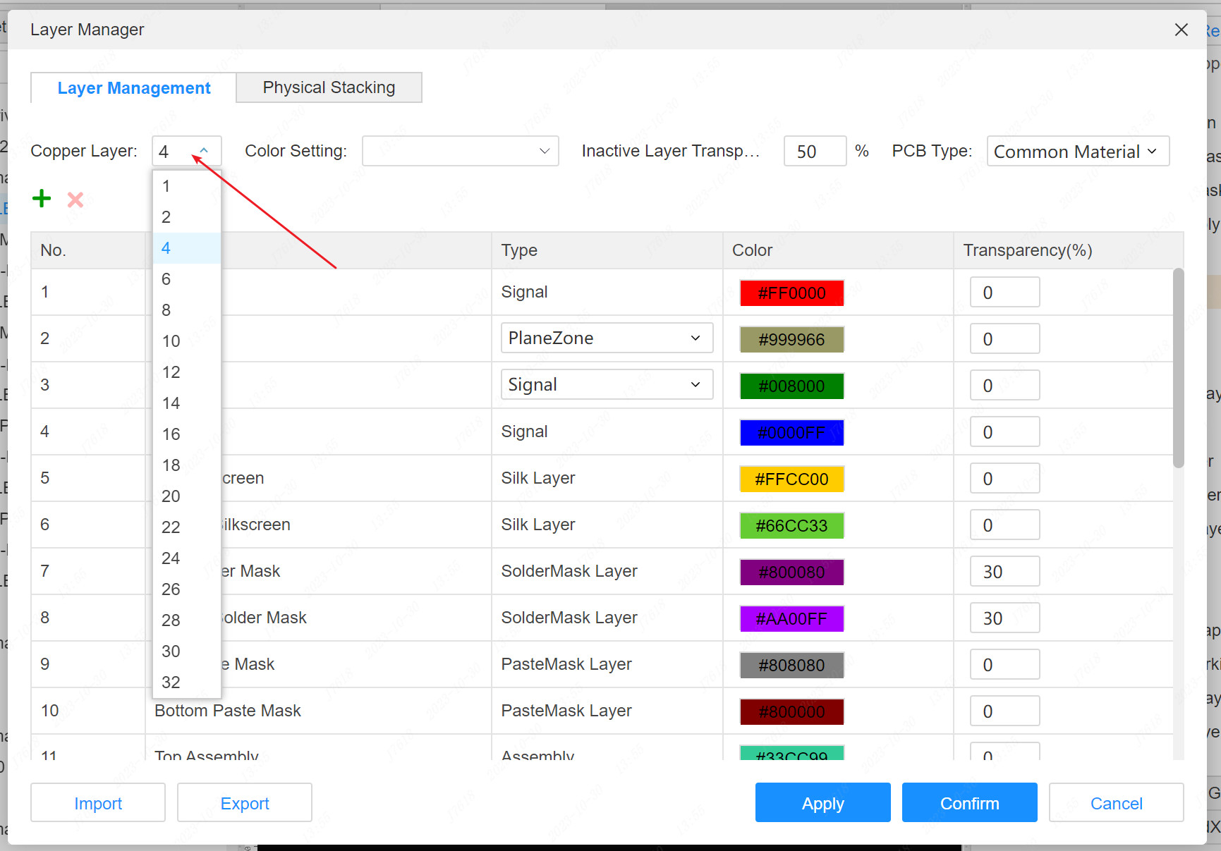
After generation, the layer manager page will have two more layers
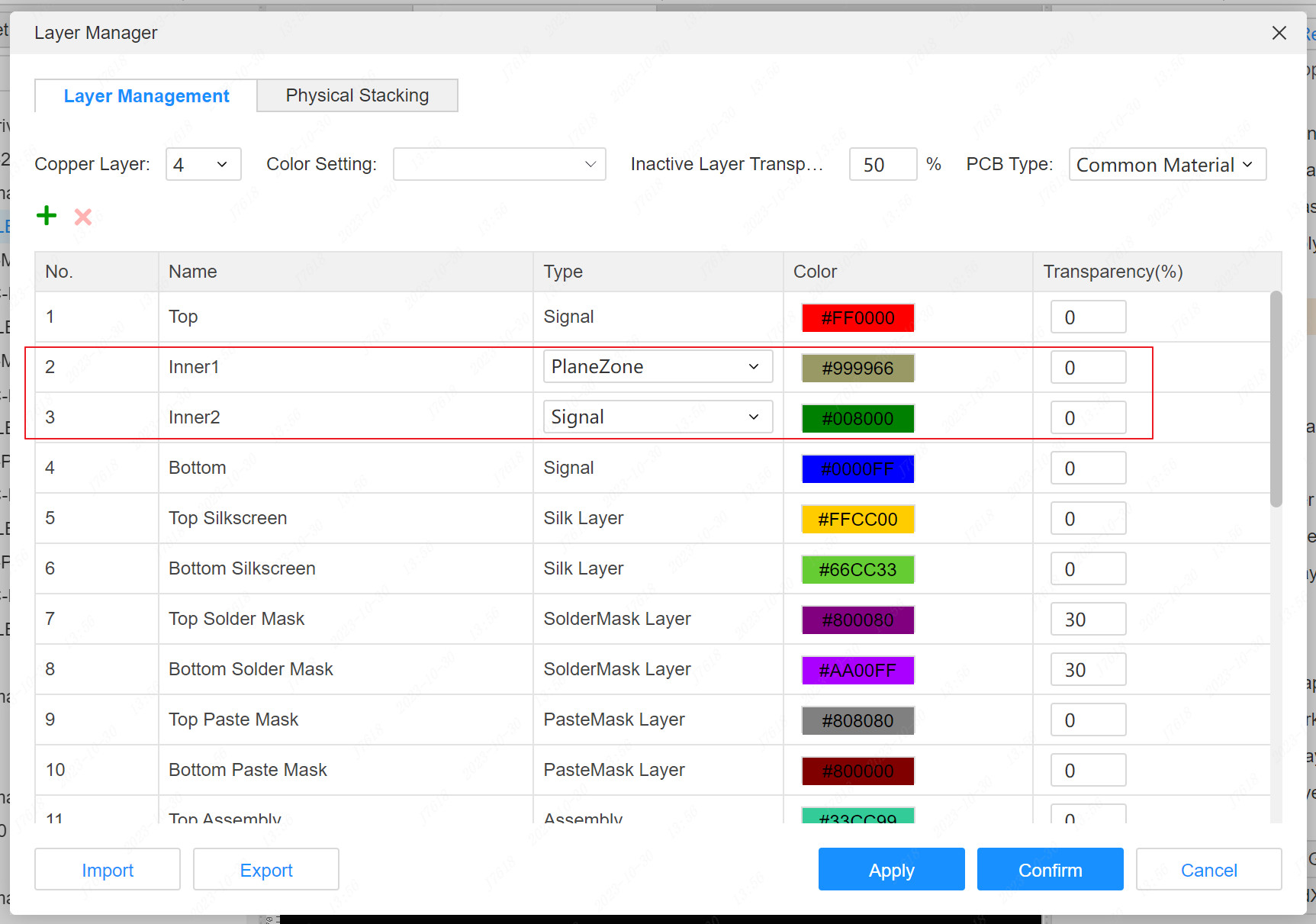
The newly added layer type can be modified, which can be modified to the signal layer and the internal plane layer. The copper of the printed board is retained where the lines are drawn, and the copper deposits where there are no lines are removed. Such as the top layer and the bottom layer, the signal layer is the positive film.
signal layer
- Signal layer: It is also a positive layer. The pcb signal layer is the same copper conductive layer as the top and bottom wiring, but it is a wiring layer sandwiched between the top and bottom layers.
Signal layer
Internal plane layer
- Internal plane layer: Also known as the plane layer or the negative layer, it is the internal power supply and ground layer (and is connected to each layer through through holes), and the internal plane layer is divided by "line" primitives. Negative film effect: Where the lines are drawn, the copper coating of the printing board is removed, and the copper coating where there are no lines is retained. Traces or other objects placed on these layers are copper-free areas, ie this working layer is negative. The internal plane layer of EasyEDA Pro is drawn in negative film mode, but it is positive film output when outputting the Gerber file, please pay attention.
- Note: The professional version does not support automatic reconstruction of the internal plane layer, you need to select the internal plane measurement to manually rebuild.
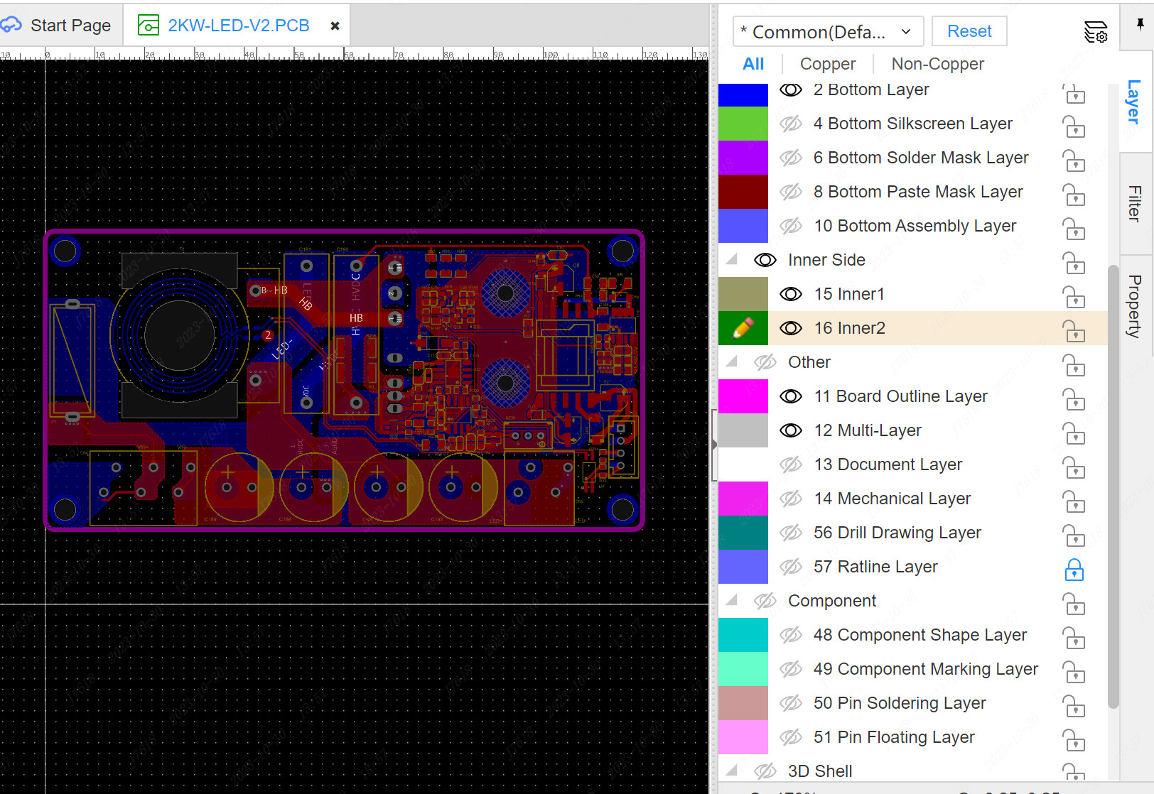
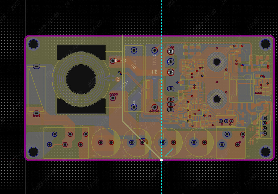
In the editor, there is a clear difference between the internal plane layer and the signal layer
Internal plane layer
The inner plane layer is like a piece of copper, which can be networked and divided.
PlaneZone Property
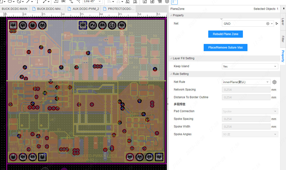
Switch to the internal plane layer and click the copper skin. On the right panel on the right, you can switch the attributes of the internal plane layer.
net:After setting up the network of each block, rebuild the internal plane layer. The copper skin of the block will be connected according to the corresponding network to avoid objects of different networks.
Rebuild Plane Zone:After segmenting the block through the lines, click the entire copper skin. After the function is rebuilt, it will be divided into multiple blocks.
Place/Remove Suture Vias:Place and remove the Suture Vias within the copper leather range of the plane zone.
Keep Island:After it is set, it will be retained without any block of the same network object.
Rule Setting:After switching the net rule, the correspondence of the corresponding network in all internal plane layers will be changed together.
Split the inner plane layer
To divide the inner electric layer, you need to use a broken line to divide it, you cannot use a wire, and after the division is completed, you need to manually rebuild the inner electric layer or the shortcut key Shift+B to rebuild all copper
The divided inner plane layer can set up multiple networks.
Note: The wire drawn by dividing the inner plane layer must be a complete closed loop.
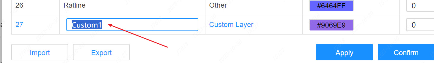
Add custom layer
easyEDA supports the creation of up to 30 custom layers. The custom layer is generally used for additional information recording, function and document layer, mechanical layer, and assembly layer similar.The custom layer does not export Gerber default, does not participate in physical production, you can use custom export when exporting Gerber, you can choose whether to export.
Click the plus number icon above the list to create a custom layer.
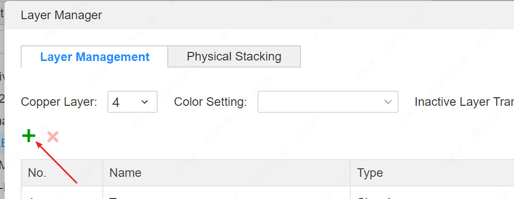
The name of the custom layer can be customized
Layer definition
EasyEDA Pro supports clear layer definition, which can refer to the following layer type and its role.
- Top/bottom:The copper foil layer on the top of the PCB board and the bottom surface is used for signal wiring.
- Inner layer:Copper foil layer, signal wiring and copper.It can be set to the signal layer and the internal plane layer.
- Top silkscreen layer/bottom silkscreen layer:The white character layer printed on the PCB board.
- Top paste mask/Bottom paste mask:This layer is a layer used for steel mesh for pad pads to help welding and determine the area size of the tin paste.If the board does not require a patch, this layer has no effect on production.Also known as the welding layer when the main film process.
- Top solder mask/Bottom solder mask:The top layer and bottom layer of the board cover the oil layer, which is generally green oil. The role of green oil is to prevent unnecessary welding.This layer is a negative film drawing method. When you have a wire or the area do not need to cover green oil, it will be drawn at the corresponding location. After the PCB is generated, these areas will not be covered with green oil.To open the window.
- Board outline:The shape of the board is defined.Define the actual size of the board, the board factory will produce board according to this shape.In the GKO file generated in Gerber.
- top assembly layer/bottom assembly layer:The simplified outline of components is used for product assembly and maintenance.It is used to export document printing, which does not affect the production of PCB boards.
- Mechanical:The information recorded in the PCB design in the mechanical layer is only used for information recording.
- The shape of this layer is made by default during production.
- Some board factories use the mechanical layer as a border when producing by AD files.In EasyEDA Pro, the layer does not affect the frame shape of the board.
- If the mechanical layer has closed lines.When EasyEDA Pro is produced, it will use the mechanical layer as the shape of the board. If there is no mechanical layer's frame, the GKO will be used as a border (the historical impact of AD files). Pay attention to the use of the mechanical layer when designing.
- Document layer:Similar to the mechanical layer, it can be used as design -related information records to view.However, this layer is usually used in the editor, which is generated in the Gerber file and does not participate in manufacturing.
- Ratline:The display of the PCB network flying line is that this is not a layer in the physical sense. In order to facilitate the use and setting color, it is placed in a layer manager for configuration.
- Hole:Similar to the flying line layer, this layer that does not belong to the physical sense is only used for display and color configuration of the pores (non -metallic holes).
- Multi:Similar to the ratline layer, the display and color configuration of the metal hole.When the pad layer attribute is multi -layer, it will connect each copper foil layer to include the inner layer.
- Component Shape:The shape layer of the component is used in the shape of the component.Convenient and comparison with the size and physical size.
- Component Marking:The identifier layer of the component can add the special logo of the component, such as positive and negative poles, polar points, etc.
- Pin Soldering:The welding layer of the component's pins is convenient to compare the size of the packaging pad and the size of the physical pins.
- Pin Floating:The pins of the component are easy to compare with the size of the packaging pad and the size of the physical pads.
- 3D Shell Outline:When drawing a 3D shell, the frame of the shell is located.
- 3D Shell Top/3D Shell Bottom:The top or bottom layer of 3D shell.You can draw digging grooves, entities such as the entity.
- Drill Drawing:This is the information that stores the drilling table for manufacturing and production control.
- Custom:The custom layer is generally used for additional information recording, role and document layer, mechanical layer, and assembly layer.Do not use it directly for production.
Color Setting
Users can select some preset color configurations of different layers here to adapt to their habits, or save them after customization.
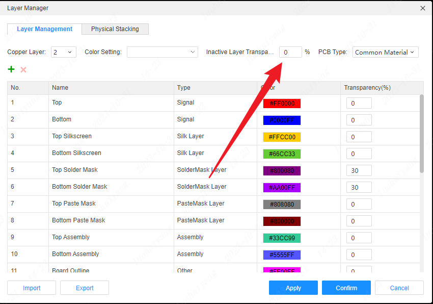
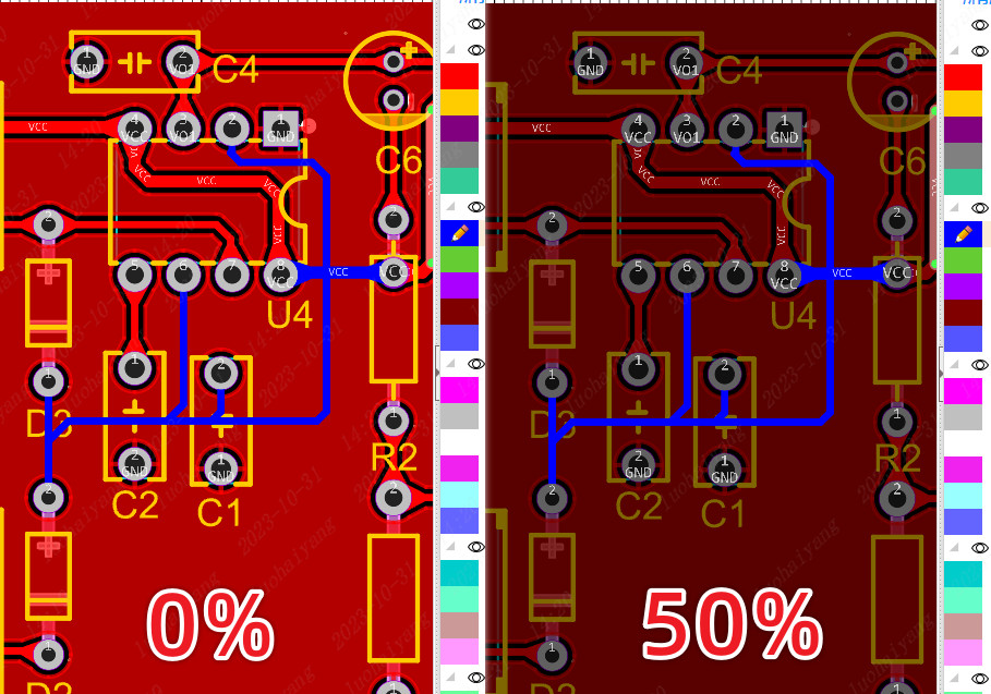
Inactive Layer Transparency
Here you can set the transparency of the contents of the inactive layer.Can improve the display effect
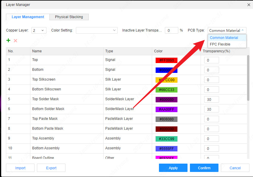
PCB Type
The type of PCB can be set here for ordinary boards or FPC soft boards. After setting to FPC soft board, the exclusive reinforcement layer of the FPC will be opened
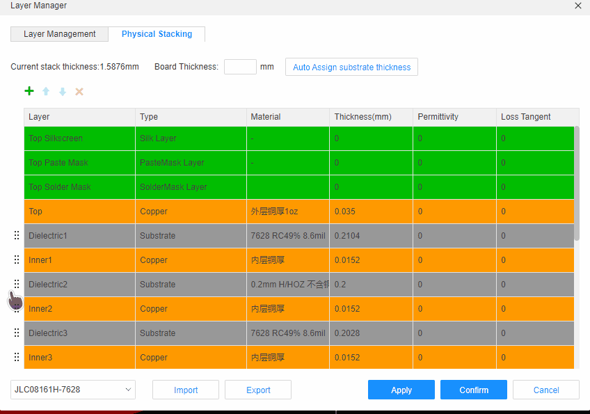
Physical Stacking
The physical stack parameters of the board can be set. At present, this parameter is only recorded, and the impedance calculation is not involved for the time being.The subsequent PCB wiring may use this parameter.
This physical stacking setting does not affect the export of Gerber. When placing an order, you need to re -select the stack parameters for ordering, but the setting can affect the thickness of the substrate medium of the 3D preview, the exported 3D file and ODB++ file.
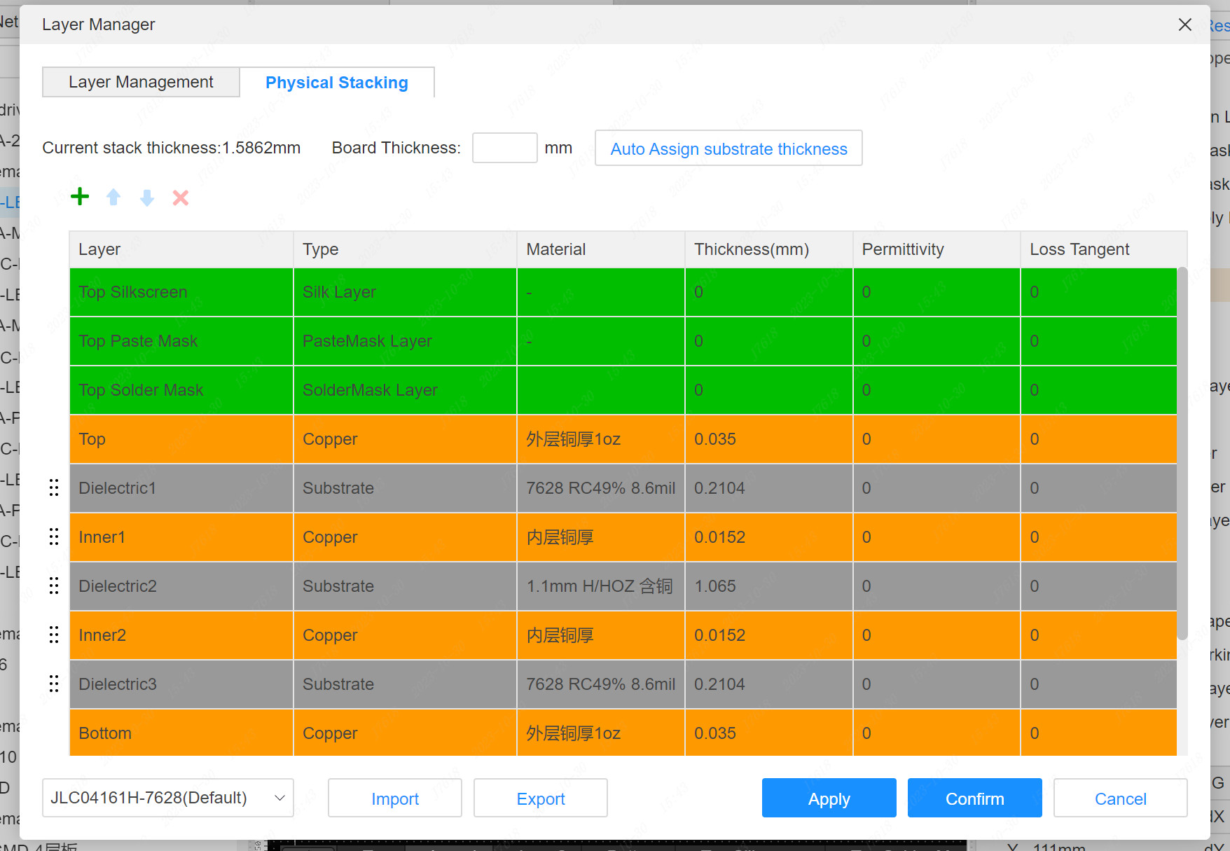
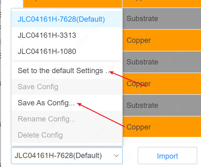
Click the drop -down menu in the lower left corner to switch the layer pressure configuration of different layers. The system provides a commonly used layer under the default of several commonly used layers.
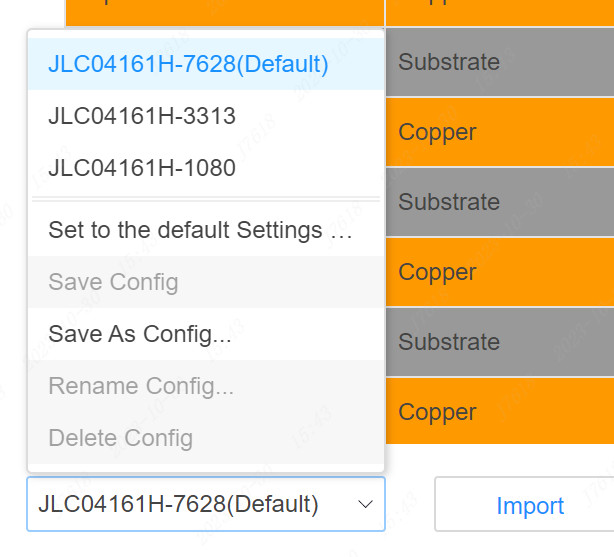
You can also set your own common layer pressure configuration under different layers of boards, and the default configuration when setting a new PCB.
You can also drag the order of the inner layer
Drawing a single layer PCB
The copper foil layers of EasyEDA Pro are double numbers. It does not support direct drawing of a single-layer PCB. You can achieve the purpose of drawing a single-layer by two methods:
method 1:
- Place and route directly on a single layer (top or bottom) without placing vias.
- If you have a footprint with multiple pads, there will be copper on the top and bottom layers. At this point, you can find out the footprints corresponding to all the multi-layer pads, right-click to edit the footprint - apply the current PCB, change the metallization (copper plating) property of the multi-layer pads to No, and then change the size of the multi-layer pads Set to "Custom" and set the diameter of the top or bottom to 0.
- After generating the Gerber, check whether the Gerber meets the design requirements.
Method 2:
- The PCB design is completed on one side, and the pads on the other side do not need to be processed to generate Gerber.
- Communicate well with the board factory when placing an order for PCB with Gerber, and make a note to only make a single-layer board.