Design Rules
Design rules are used to set the basic design principles of the PCB. Entering a safety design rule in the design rules can ensure that there will be no design problems in the design of the PCB.
Steps:
- Top Menu - Design - Design Rules
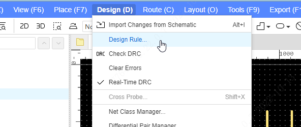
at Design Rule dialog, you can set many rules for the PCB
The lower left of the design Rules dialog box supports multiple preset process configuration switches 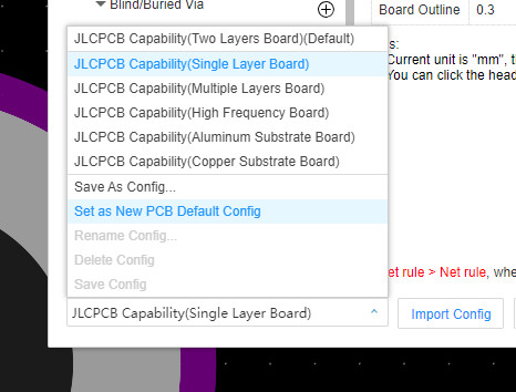
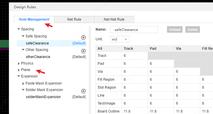
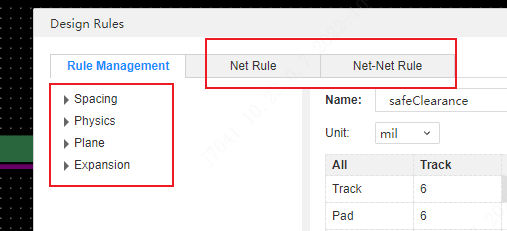
Rules management
Under the rule manager, you can add, modify, and delete rules under each type of rule. For networks without special rules, the default rules will be used.
Rules type introduction
There are currently four categories, and one or more rules are created under each specific rule
rules editing
Click the + icon to the right of the rule type to be added to add a new rule. After entering the rule name, click the mouse outside the input box to create the rule successfully.
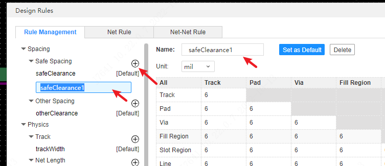
After adding a new design rule, you need to rename the rule. It should be noted that the rule name of the same type cannot be repeated.
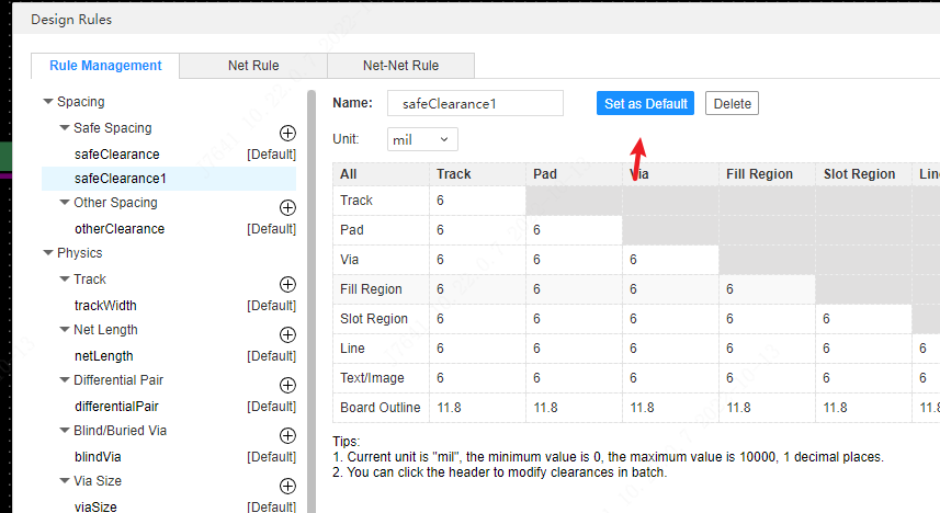
- Default rules
There is only one under the default rule type in the left column, and this rule will be pinned to the top.
If you want to set a rule as the default rule, click the Set as Default button in the rule view.
- Delete rules
Non-default rules support deletion. Click the delete button in the rule view to be deleted to delete the rule.
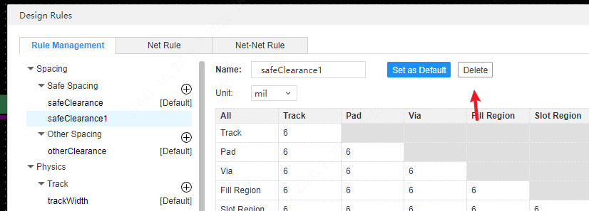
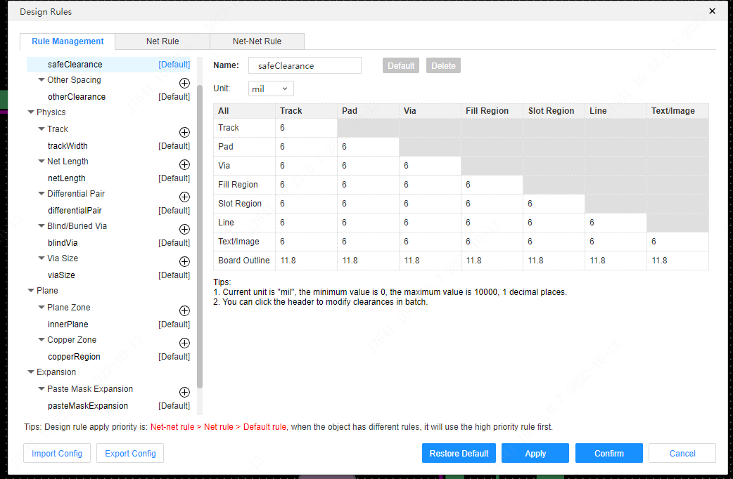
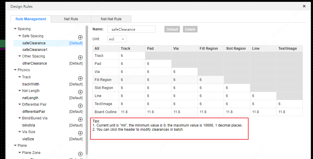
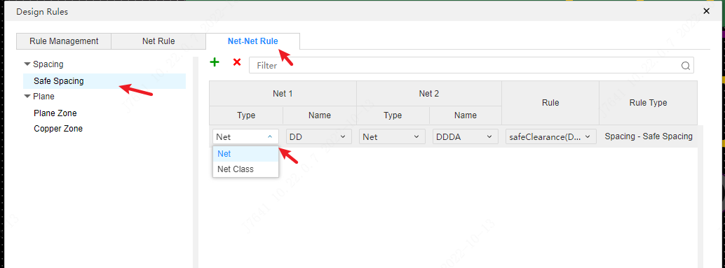
Safe spacing rules
The safe spacing table allows you to set spacing requirements between two different network elements.
Double-click any table to modify the value of the rule.
Click the name at the top to edit values in bulk.
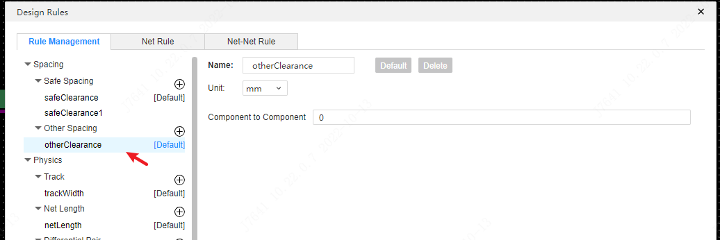
Other spacing rules
Currently, the device-to-device spacing rule is supported, which is detected by a rectangle surrounded by the overall outline of the component.
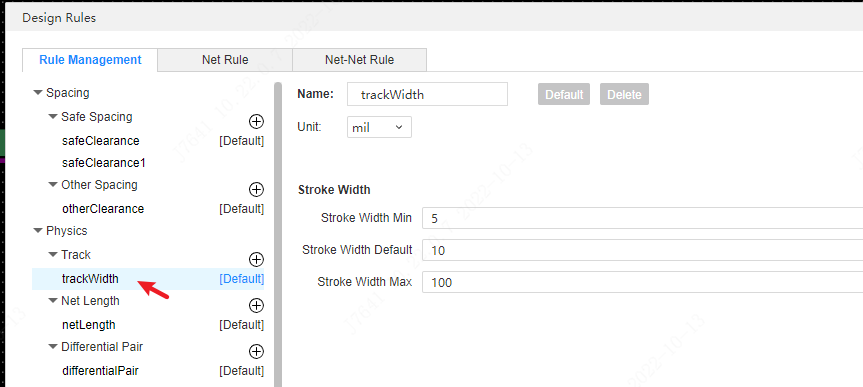
Track Rules
Minimum, default, and maximum line widths for wires can be set in a wire rule. If the line width of the wires in the PCB does not meet the range from the minimum line width to the maximum line width, it will be detected by DRC. The default line width refers to the default line width taken for each routing, but when routing starts from a wire, the line width of that wire will be used as the starting line width.
Network length
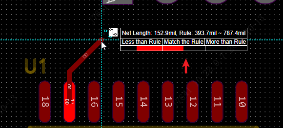
The net length rule is used to set the overall length of the checklist net trace. This rule cannot be applied to design constraints, but can be viewed during wiring.
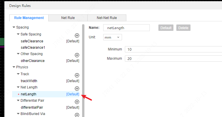
There will be an indication when the line meets the set rule length. In the case of conforming to the rule, the indication will be marked in green, and if it is larger or smaller than the rule, the indicator will be marked in red.
Blind and buried via rules
Blind and buried vias are usually used in the design of multi-layer boards. Before adding blind and buried vias, it is necessary to determine whether the designed PCB has been set to multi-layer. If it is not set, it needs to be set in the Tools - Layer Manager, to enable more copper layers.
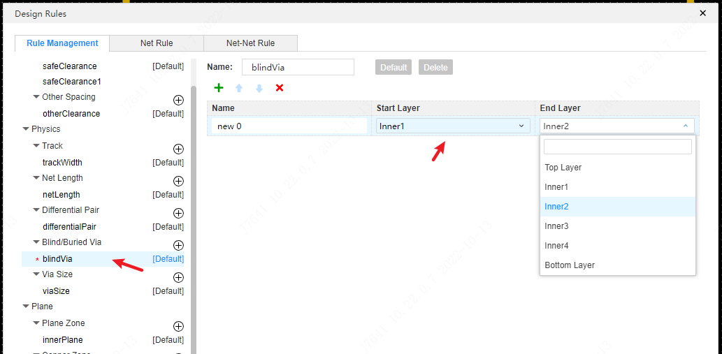
If the PCB needs blind and buried vias, it needs to be added in the design rules first.
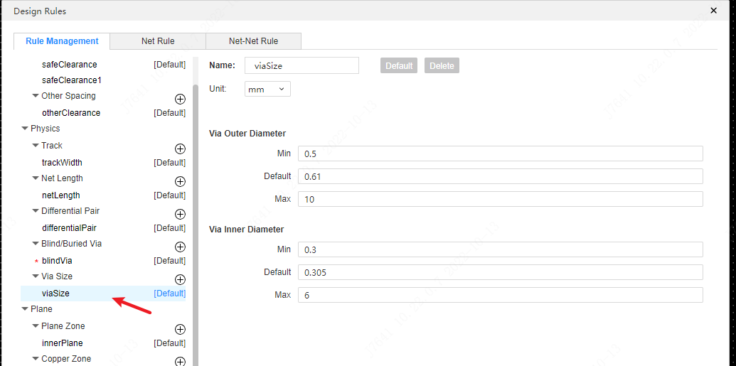
Via Size Rules
The minimum, default and maximum dimensions of the via OD/ID can be set in the via size rule. If the via size in the PCB does not meet the minimum to maximum range, it will be detected by DRC. The default aperture refers to the default size taken each time a via is placed.
Plane Zone Rules
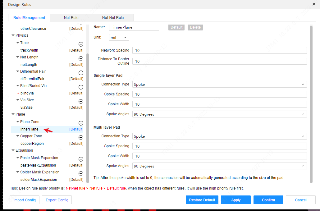
- Network Spacing: Set the spacing between the copper filling and different network elements when placing copper.
- Distance To Border Outline: Set the spacing from copper filling to border and slot area.
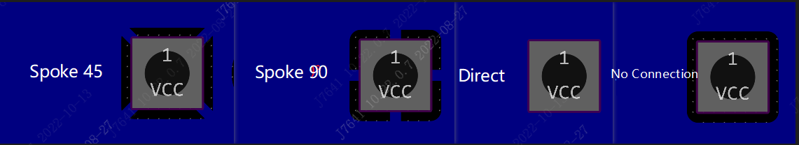
- Pad Connection Type: It is divided into divergent and direct connection. When set to divergent, divergent line width and divergence spacing can be set respectively.
- Spoke Spacing: Set the divergence spacing between the pad and the copper.
- Spoke Width: The setting of the divergence distance between the copper skin of the connection pad wire.
- Spoke Angles: Supports the setting of the angle of the inner copper layer connection method.
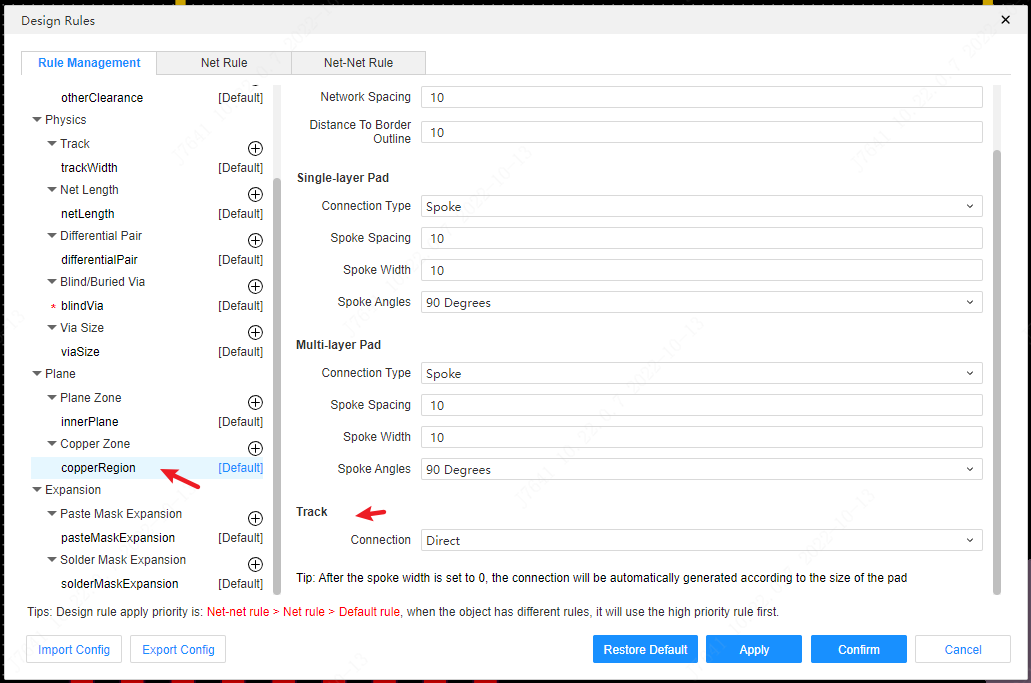
Copper Zone Rules
The copper laying rules are the same as the plane zone rules, and will not be repeated here.
Note: When the copper-plated pad divergence line width is set to 0, the connection line width will be automatically generated according to the size of the pad.
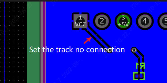
Compared with the internal electrical layer rules, copper laying has an additional wire connection method setting, which supports setting it to no connection. When set to no connection, the copper will not be connected to the wire, and it will not appear that the wire is covered by the copper.
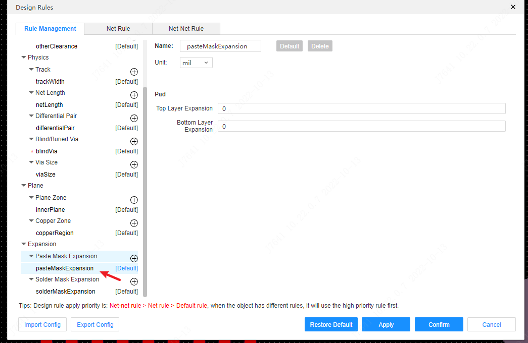
Paste Mask Expansion Rules
The paste mask expansion is used for the pad of the SMD footprint. When the paste mask expansion property of the pad is set to general, the mask expansion in the design rule will be used as its flux.
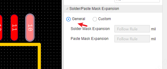
when you select a pad at PCB, you can set its solder or paste expansion value
Solder Mask expansion Rules
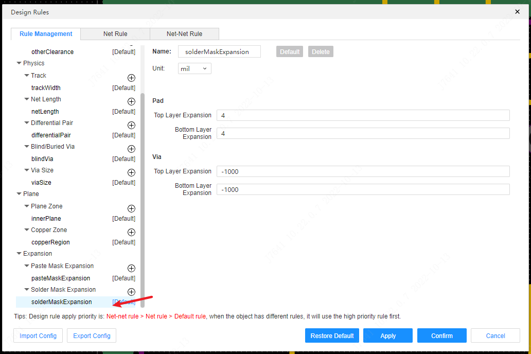
The solder mask expansion of pads and vias can be set separately in the solder mask expansion. If you do not want to open the vias, set the solder mask expansion data to a number smaller than the aperture (such as -1000mil)
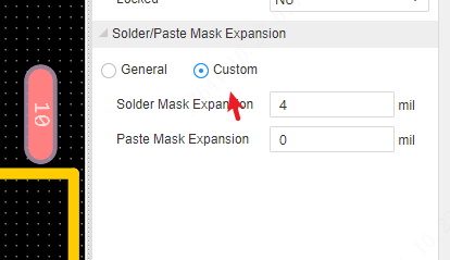
Similar to mask expansion, the solder mask expansion of the default pads and vias follows the rules
If you need to customize the solder mask of a pad or via, you need to modify its solder mask expansion parameters in the properties panel
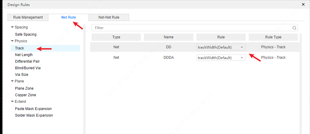
Network Rules
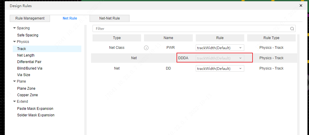
In the net rules, you can assign rules to all nets of the current PCB. First, select the type of rule you want to assign in the left tree, and then view the network list in the right view. By default, all networks are under the default rules. If you need to modify the rules of a network, directly in the drop-down box of the corresponding network rules Just switch.
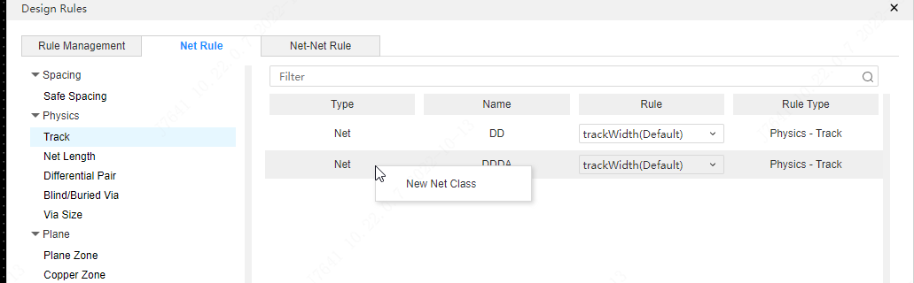
In the network rules, the function of quickly creating a network class and adding a network class is provided. Right-click in the network list and select the function of creating a new network class to create a new network class.
After the new one is created, the network class will be pinned to the top.
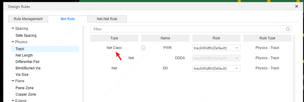
Assign a design rule to a net class, and all nets under the net class will become this rule
Network - Network Rules
Supports setting rule constraints between two different network rules, and supports rule settings for safe spacing, internal electrical layer, and copper laying.
Networks, or network classes, can be set up and assigned different rules.
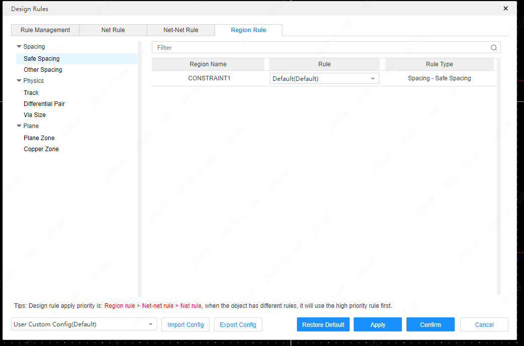
Region Rule
Support the rules in the constraint region in the canvas, support safe spacing, other spacing, track, differential pair,via size,plane zone, and copper zone.
Different rules can be allocated for different restraint areas in the canvas.