PCB Setting
Canvas property
After opening the PCB, you can set the commonly used settings on the right attribute panel. These settings are set on the top menu, right -click menu, and filtering TAB can be modified.The setting parameters can be saved into the PCB. The next time you open the PCB, the parameters of the settings are given priority.
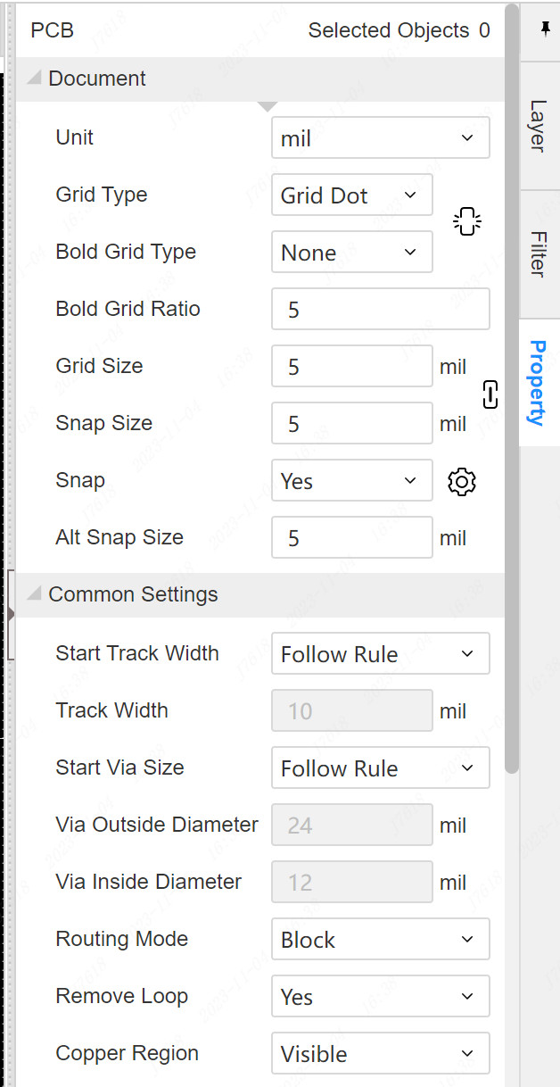
PCB preference settings
Many of the operation -related settings in PCB can basically set up -PCB -general settings to view and modify its attributes.
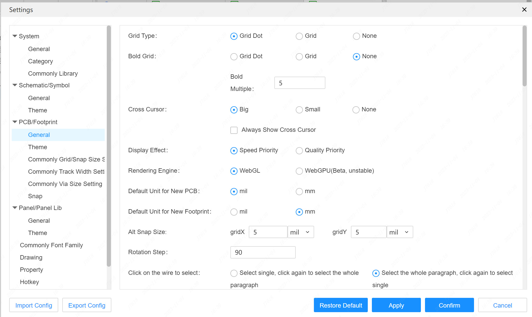
Grid Type:Grid Dot,Grid,none
Bold Grid:Grid Dot,Grid,none.After the bold mesh setting, the display effect will be thicker than the ordinary grid. You can adjust the color and transparency in the PCB theme settings
Bold Multiple:For the ordinary grid size of each thick multiplayer, the bold grid is displayed
Cross Cursor:Change the size of the cursor in the PCB editor.
Always Show Cross Cursor: After the selection, the mouse will always be the shape of the cross cursor.
Display Effect: The priority will improve the performance of the editor, but the quality decreases.The quality priority is to open anti -aliasing. After opening, the display will be relatively smooth and have certain demand for computer configuration.
Rendering Engine:Webgl, webgpu.WebGPU is currently a test version, and the performance is unstable.
Default Unit for New PCB: Amend the new PCB unit here.
Default Unit for New Footprint: Modify the newly -built unit here.
Alt Snap Size: ALT adsorption size (applying this parameter according to ALT adsorption during drawing)
Rotation Step: The angle setting of the device rotation.
Click on the wire to select: Divided into selecting a single segment, click the entire section and select the entire section, and click again to select the single segment.Here will affect the selection range of the first selected wire and contour object, and click again to switch to another range of selection.
Copy/Cut: Select the reference point when copying the object.
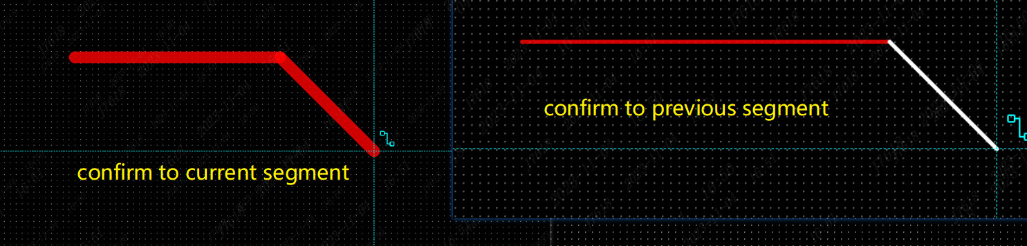
Confirm track segment while routing: Each time you add a wire segment when the wiring The quantity is confirmed to add multiple paragraphs at one time in the current paragraph, and confirm that the previous paragraph adds a paragraph
End primitives drawing: To set the draw mode, right -click is to end the drawing or the right -click menu. Ctrl+right -click will be the opposite behavior.
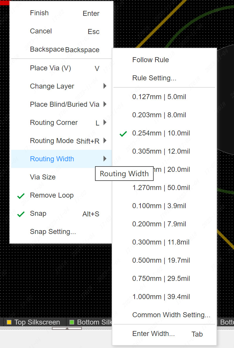
Add via method while route: Add at the previous turning point, and fixed the position of the perfunction at the previous wiring turning point position; add the current turning point, follow the mouse to move, and confirm the location after adding a new inflection point.
Rotation Objects: Rotate the single object. When multiple objects are selected for rotation, each object is rotated according to the respective center; the overall rotation is selected.
Start Track Width for New Document: Set whether the width of the wire when the new PCB is set up follows the rules.
Default font type for component properties: After setting the schematic diagram to the PCB, the component's attributes such as the default font type and high attribute information displayed in PCB.
Start Via Size for New Document: Whether the perforated size follows the rules when setting a new PCB.
Show Number or Net
- Show Pad Number: Show the number of the pad of the device.
- Show Pad Net Name: Display and hide the network of pads of the device.
- Show Track Net Name: Hide and display the network on the wire.
- Show Via Net Name: Display and hide the network of holes.
Real Time Display
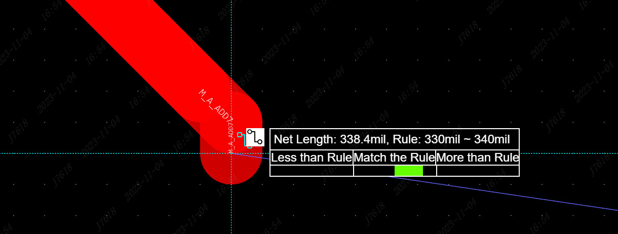
- **_Display Real-Time Net Length While Route or Stretch Track_**: After turning on, when the wiring, drag, stretching wire, and long adjustment, the network length information is displayed in real time. If the network sets the network length rules, it will also show the network length range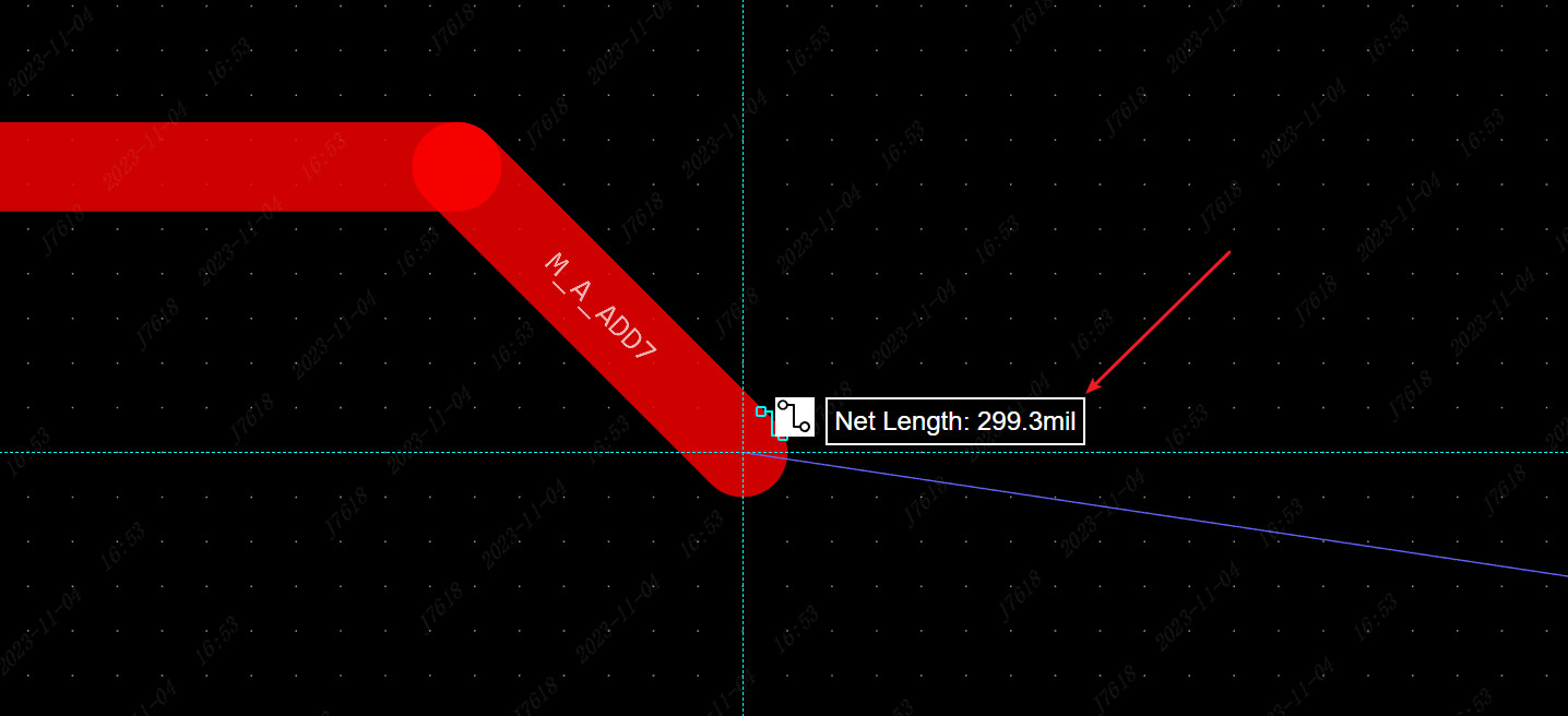
- **_Display Real-Time Differential Pair Length Tolerance While Route or Stretch Track_**: After turning on, when the differential pair, drag, stretch the wire, and adjust the long adjustment of the different time, display the differential pairs of length error information.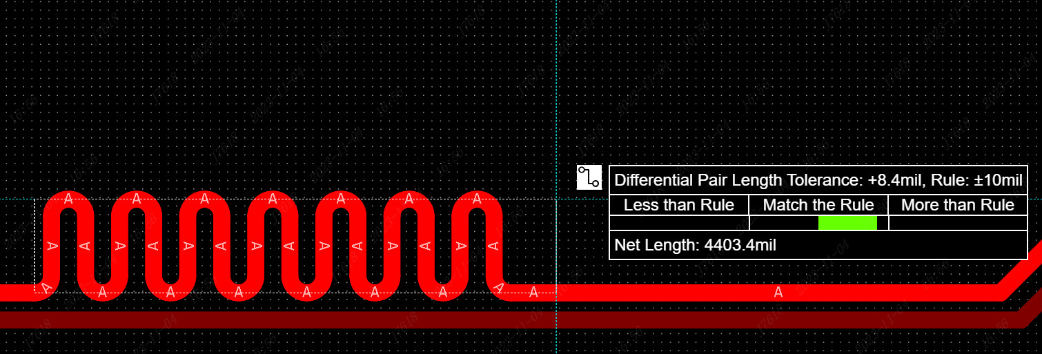
- **_Draw Using Dynamic Input Box_**: Draw a folding line or polygon in the current free angle of the line and the angle of the arc free angle, the rectangular, and the round mode. The dynamic input box will appear in this function. The directly input parameter is used to lock the parameter according to the TAB or ENTER.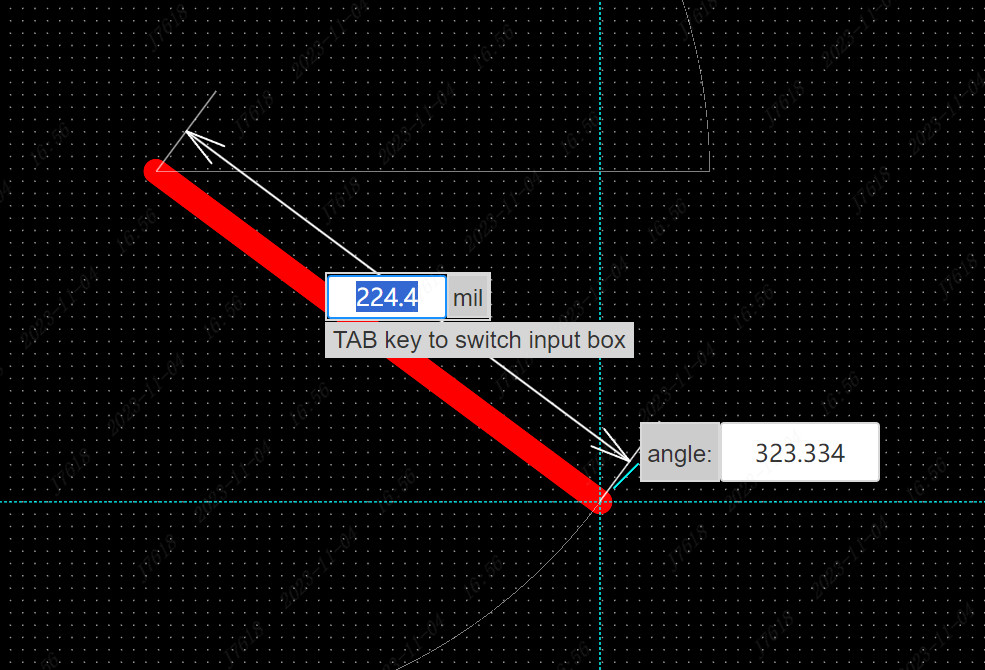
Mouse Hover - Highlight the Net When Hovering Over the Net: When the mouse hovers on a certain wire, pad, and pores, the wires, pads, and pores of the entire network are highlighted. - Highlight Object While Cursor Hover Object: When the mouse hovers at a certain object, Gao Liang is high. At this time, holding the object in the mouse selection will be the same as the object of Gao Liang. - Display Object Property While Cursor Hover Object: When the mouse hovers at a certain object, some attribute information of the object is displayed.
Route
- Prefer Place Blind/Burried Via while Change Layer on Routing: When the pores are placed in the wiring switching layer, set the perforated or blinded holes for priority.
- Auto Change Layer While Routing Vias: After turning on, add holes during the wiring process and automatically switch to other layers at the same time.
- Automatic fan-out when end of routing: After turning on, when the chip pin wiring is turned on, it is given a distance from the pad.
- Terminate Routing Automatically: After clicking the other map of the same network, the wiring is ended, that is, the wiring is over.
- Assign Net for Free Track: When drawing a network -free wire, it will automatically allocate a new network for the free wire and the connected pads after ending the wiring.
- Add Teardrop Automatically: Draw a wire, drag a wire, pad, and a hole, and automatically add tears.
Drag/Move
- Ctrl drag to copy: Press and hold the ctrl key to drag the object, you can copy the new object。
- Cursor snaps to center while dragging pads/vias: Drag the pads/perforated, and the cursor automatically adsorb to the center and follow the mouse.
- Cursor snaps to origin while dragging footprints: Drag the package, automatically adsorb the cursor to the heart and follow the mouse.
- Align in adjacent footprint/pads when mobile footprint/pads: Drag the packaging/pad, if there are other pads and packaging next to it, it will automatically adsorb to the position of the alignment boundary when moving to its boundary.
Move the footprint, wire's following way: When moving the device, the wire follow -up method is set.
Move the Via, wire's following way: When moving the holes, the wire follow -up method is set.
Other
- **_Show Scale Ruler_**: Close and open the scaling ruler below the top shortcut bar.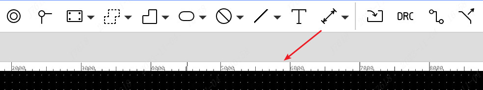
-   **_Check Net Connections Before Generating the Fabrication File_**: When exporting the Gerber file, check whether the connection of the PCB network is completed.
-   **_Check DRC Before Generating the Fabrication File_**: When exporting the Gerber file, check whether the DRC prompt is checked.
-   **_Reserve Designators when Pasting_**: Stick the copy of the device to PCB, keep the original number.
-   **_Using JLC color silkscreen technology_**: After enabling, you can use colored silk print -related functions.
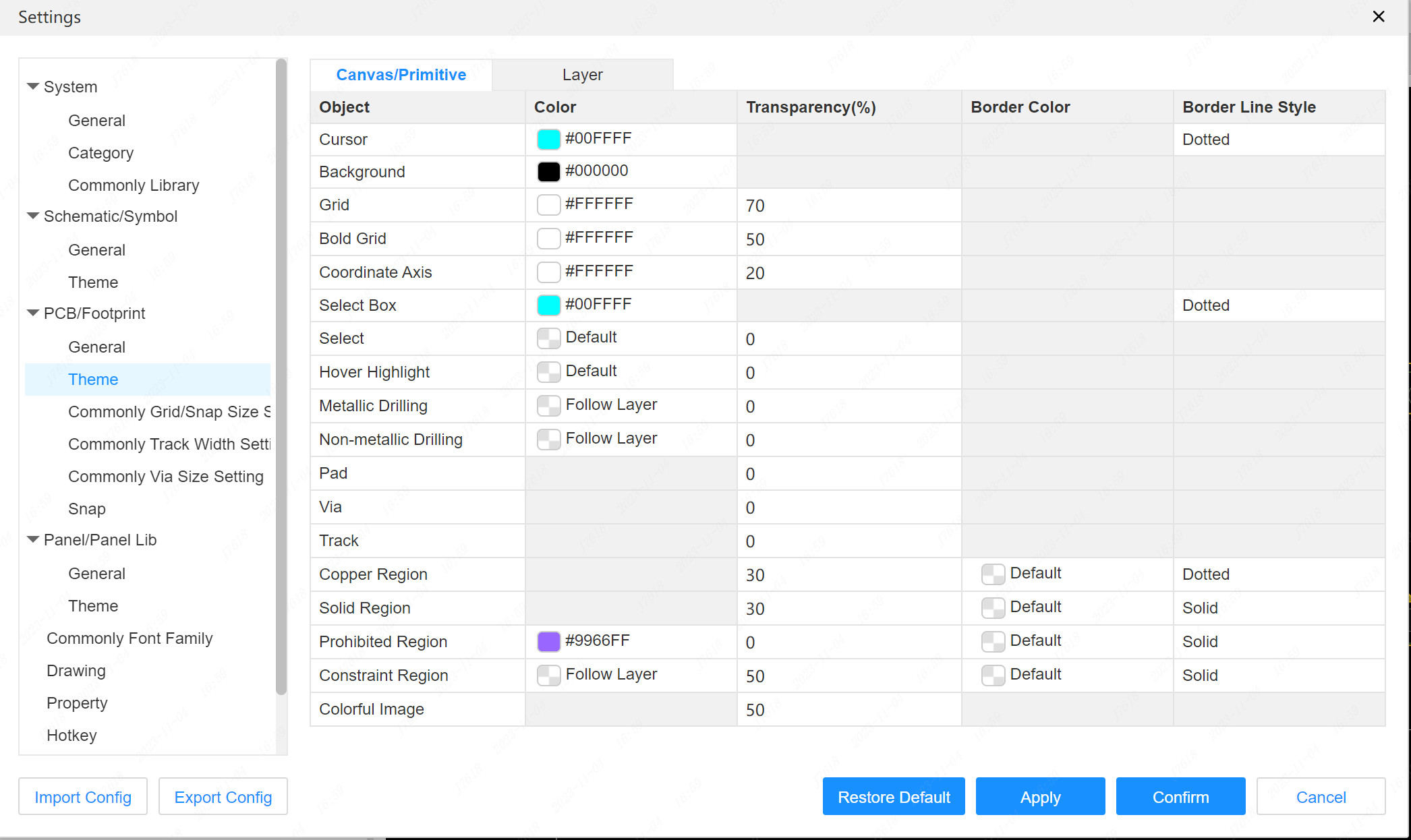
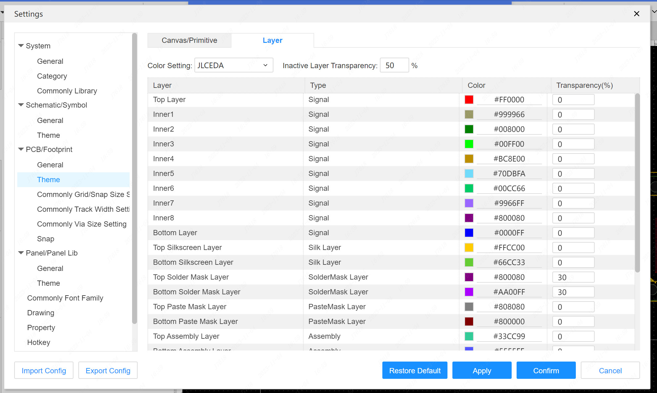
Theme settings
PCB interface theme settings, users can set some color configurations of the PCB interface according to their personal preferences, or they can choose the theme of other PCB software.
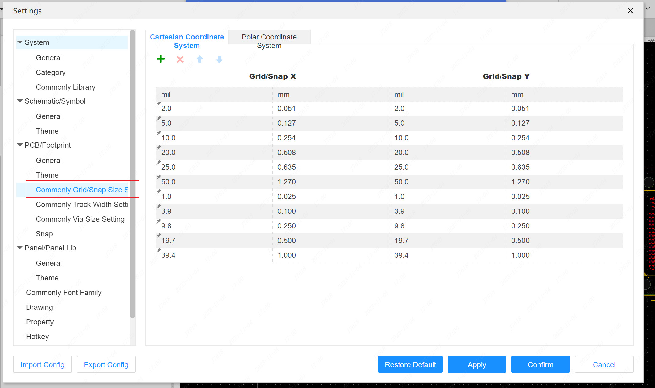
Commonly grid/snap size settings
Set the size of the common right -angle coordinate system and polar coordinate grid, which is convenient for switching the size of the grid display when wiring.
Common track width settings
Set the common wire width of the wire, and you can quickly switch the width of the wire when the wiring. 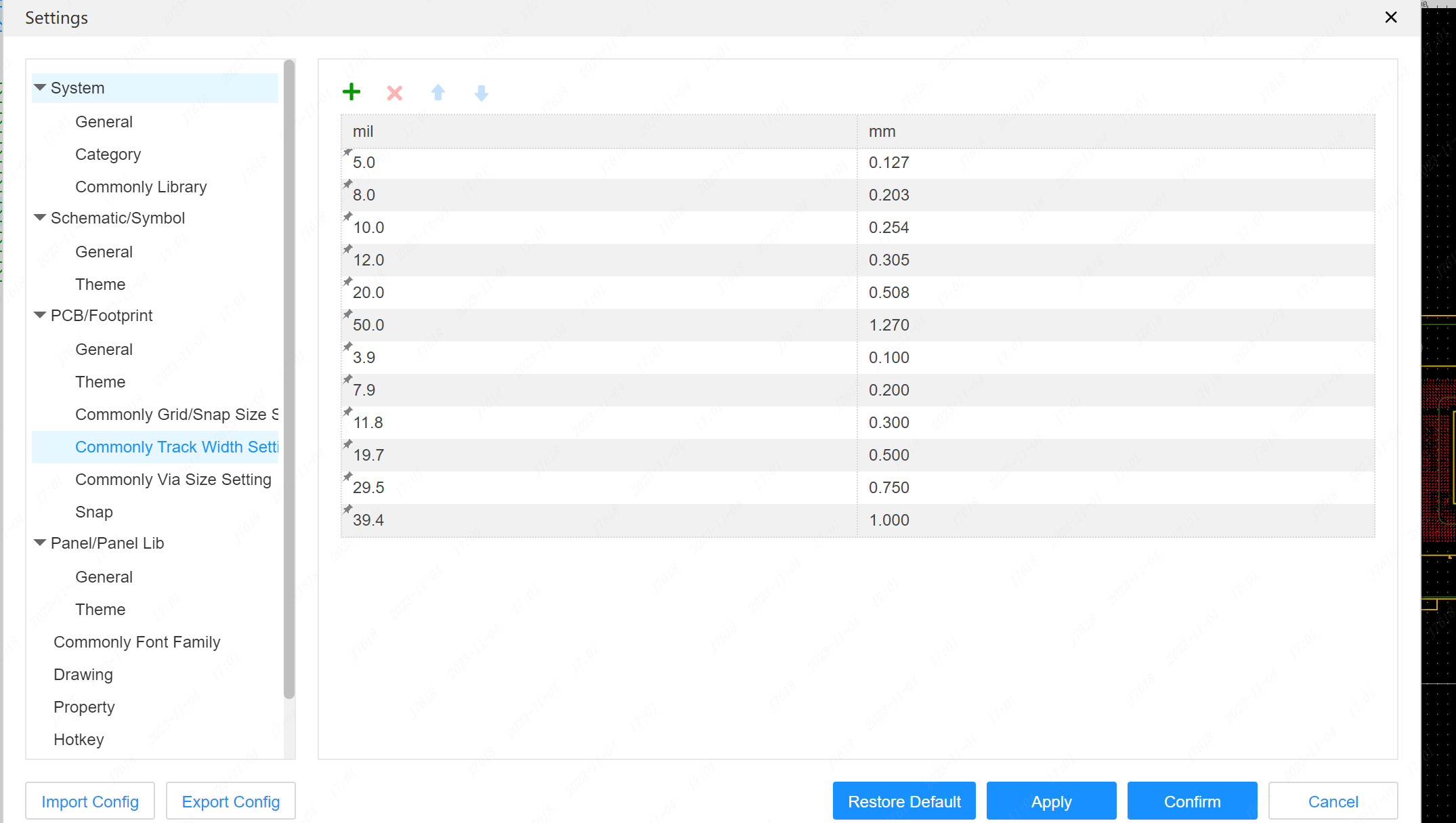
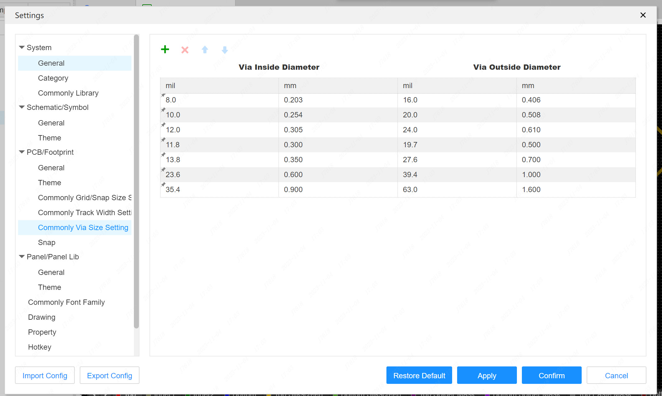
Common via size settings
Set the commonly used perforated size, which can be quickly switched to the hole when placing the hole.
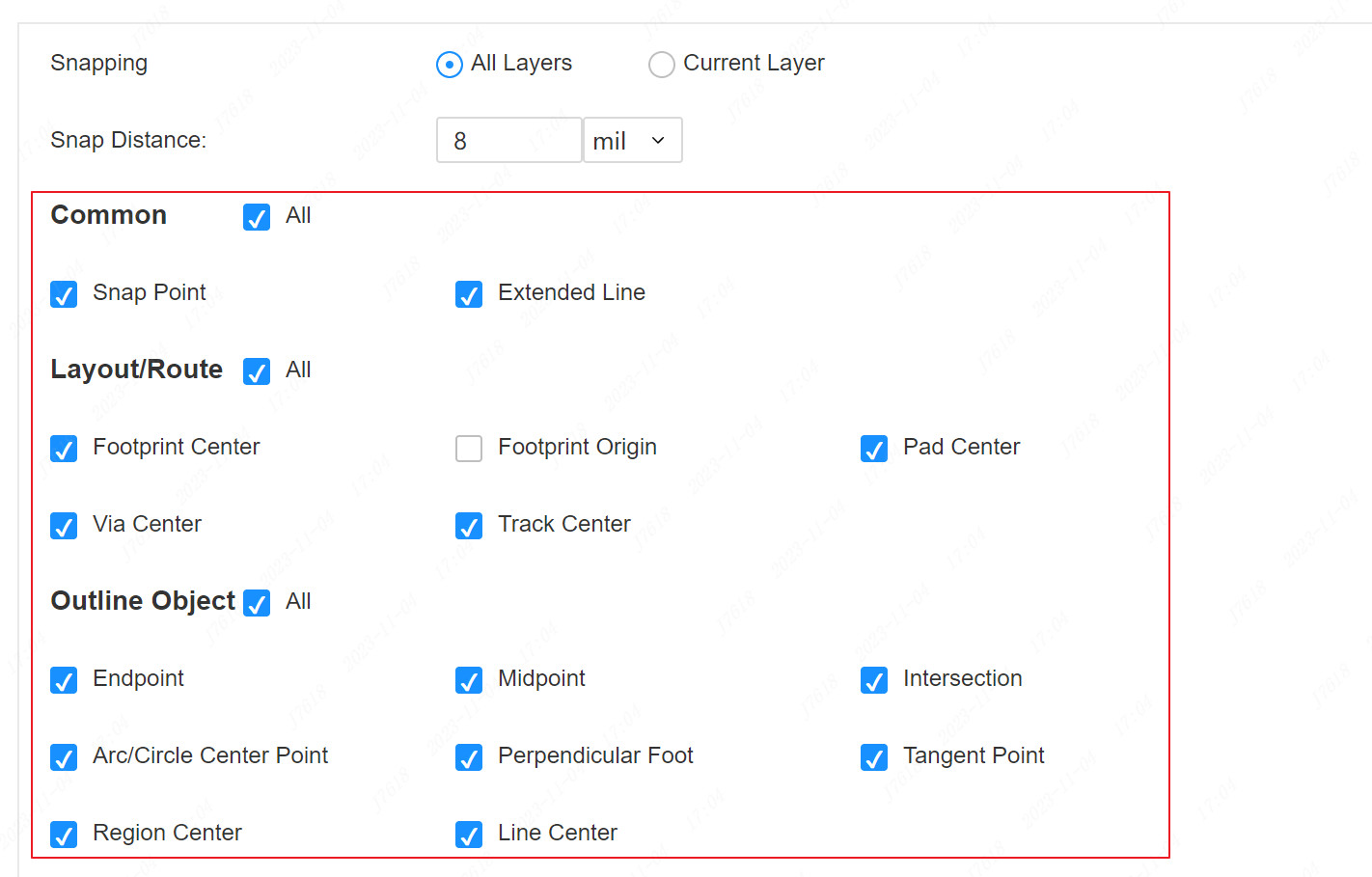
Snap
*Snapping: You can set the adsorption only to take effect on the current activation layer, or take effect on all layers.
Snap Distance: When the cursor moves to the adsorption point adsorption distance, it is automatically adsorbed to the adsorption point.
Adsorption item settings: You can check the adsorption object you need here
Add commonly used fonts
Support setting your own commonly used fonts.These fonts need to be installed on the local computer before being called by the editor, otherwise the editor will automatically use the default font provided by the browser for rendering.
Add custom font:
First install the fonts you need in the local computer. If you already have fonts, you can ignore this step.
Taking the Windows system as an example, find the font settings in the system settings and get the font name.You need to get the accurate display name, which cannot be the file name of the font file.
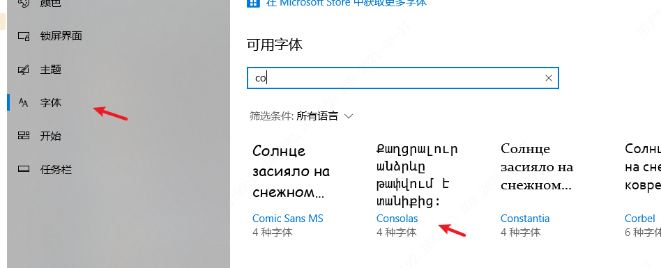
Add a font according to the font name.
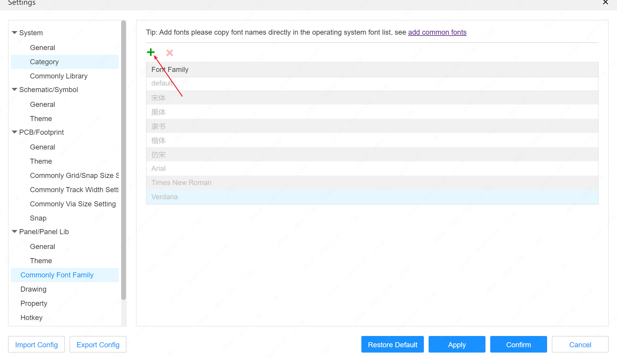
- This font can be seen in the text font switching of the schematic or PCB. At this time, the font switching can be performed.
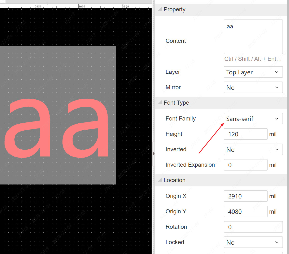
The fonts that are added can be used by schematic diagrams, panels, PCB, etc.