Import Allegro/OrCad
EasyEDA Professional Edition supports importing OrCad schematic files and Orcad schematic library files. You need to export the schematic diagram to EDIF format in Orcad first, and export the schematic library file to XML format before you can import it in EasyEDA Pro Professional Edition. Starting from v2.1, it will support importing Allegro files. It needs to use script conversion to convert Allegro to ASCII format before importing.
It is recommended to use EasyEDA Pro format converter for format conversion.
Steps
Import OrCad files
Open the OrCad software and open the schematic DSN file
In the top menu - File - Export - EDIF or Library XML, get the schematic EDF suffix file or the schematic library file XML. If you are exporting XML, you need to manually select the OLB file and output directory to be exported.
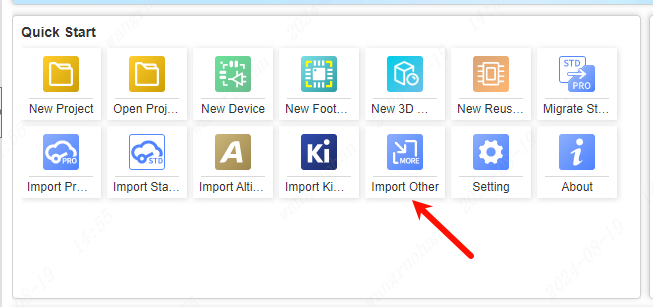
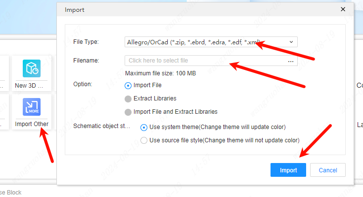
On the EasyEDA Pro start page, choose to import other
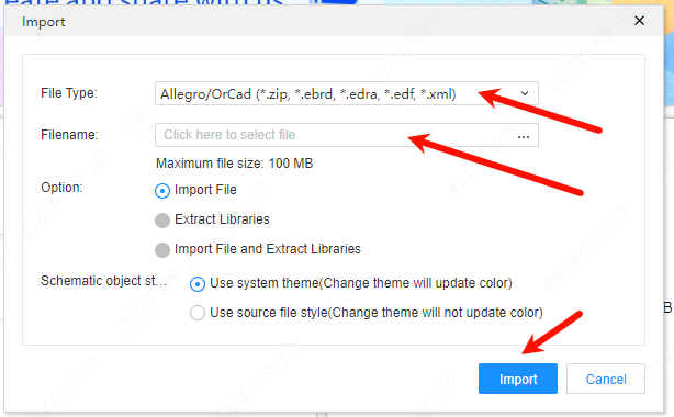
Select Allegro/Orcad from the drop-down list of the file type, select the file and import it. You can choose to import the file or extract the library according to your needs.
If the OrCad schematic diagram and Allegro's PCB are the same project, you can convert the Allegro files and compress them together in a zip archive and then import them into EasyEDA Pro. When importing, the package will be automatically associated with the device.
Import Allegro file
Since v2.1, EasyEDA Pro support to import Allegro. Because Allegro's file is an encrypted database file, you need to use one of its extraction tools to convert the database into an ASCII file. Download the conversion plug-in below, and you can export .ebrd and .edra files after installation.
Download the Allegro to ASCII plug-in:
1. Download [EasyEDA Format Converter](/en/import-export/easyeda-pro-format-converter)

2. Or download extension:
run exe to install: export-allegro-to-ascii_v3.1.zip run bat to install: export-allegro-to-ascii_v3.1_bat.zip
Install the plug-in according to the tutorial in the compressed package. Note that plugins may not be compatible with lower versions of Allegro, please verify by yourself. Double click the
install-allegro-extension.exeorinstall-allegro-extension.batto try to install the script, if install failed, you can read the Readme.txt file to install manually.Open the Allegro software, and open the Convert PCB to ASCII or Convert Lib to ASCII pop-up window in the Batch Conversion menu on the top menu.
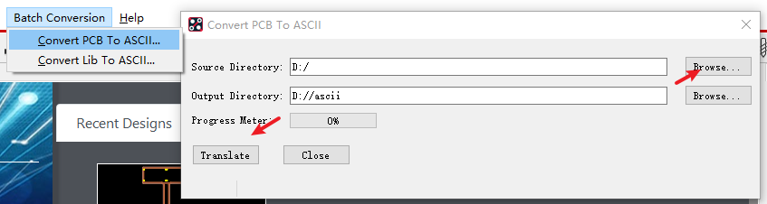
After opening the pop-up window, select the directory where the brd or dra file to be converted is located, and set the directory to be output, and click the Translate button to convert.
Find the PCB file with the suffix of ebrd in the output directory, or the package library file with the suffix of edra, and import it in EasyEDA
Batch Conversion
Batch convert OrCad
If you have a large number of Orcad schematics or schematic libraries, you can use the following plug-in for batch conversion, which will scan and convert according to the folder and subfolder you choose.
Download the conversion script: export-orcad-to-ascii.zip
Install the script after decompression. Perform the installation script according to the Readme.txt inside.
Perform batch conversion of schematic DSN files or schematic library OLB files according to the tutorial.
After the conversion is completed, find the file in the output directory, and then import it in EasyEDA Pro. If the OrCad schematic diagram and Allegro's PCB are the same project, you can convert the Allegro files and compress them together in a zip archive and then import them into EasyEDA Pro. When importing, the package will be automatically associated with the device.
Batch convert Allegro
If you need to convert Allegro files to ebrd or edra format in large batches, you can use the conversion plug-in provided above to perform batch conversion after selecting a folder.
The plug-in will automatically traverse the subfolders and all brd files or dra files under the folder. It will take a long time for batch conversion, please wait patiently.
Precautions
- Because the Orcad schematic diagram does not include the PCB, so far after importing the Orcad schematic diagram to EasyEDA Pro, the package attribute of the component will be empty, and the package needs to be re-bound. This is because the package binding design is different from that of Orcad. EasyEDA Pro needs to be associated and bound, and cannot be associated by entering the package name.
- The graphics element design of Allegro is different from that of EasyEDA Pro, and there may be differences in details, such as copper laying, thermal welding of pads, square holes, porous pads, etc., will be imported according to the graphics of EasyEDA Pro. Meta properties are automatically adjusted.
Difference before and after import
| Graph Element/Layer | Allegro | EasyEDA Pro | Supplementary Explanation |
|---|---|---|---|
| Layer | PLACE_BOUND_TOP, PLACE_BOUND_BOTTOM | Component Outline Layer | Import the professional version of the component outline layer. |
| Layers | - | DOCUMENT | Some layers whose role is unknown are resolved to the document layer |
| Layer | - | Custom Layer | Layer not corresponding in Board Geometry |
| Font | Stroke Font | Default Font | Slight Deviation |
| Pad solder mask, solder flux | can be any graphics | solder mask, solder flux expansion | - |
| Pad number | Position can be set | Ignore the position information | Display in the center of the pad |
| Square drill holes | - | Replace with round holes | - |
| - | Drilling symbol | - | This symbol is not required |
| Line width | The line width of some primitives that need line width is 0 | - | Set the default line width to 1mil |
| Multiple holes in the pad | - | Only one hole is reserved | Multiple holes in the pad are not supported at the moment |
| Pad inner layer graphics | Each inner layer graphic element can be defined separately | The inner layer graphics are the same | Take the default internal graphics in Allegro and import |
| Hot Air Pad | Thermal Pad | It can be replaced by thermal welding rules | Insufficient information in the package file, use the default rules |
| Isolation Pad | Anti Pad | It can be replaced by the inner layer network spacing rules or forbidden areas | It is not analyzed in the package file because the scene is not applicable |
| Inner layer graphics in the package | Corresponding to PCB inner layer graphics with the same name | Corresponding to PCB inner layer graphics with the same layer id (physical stacking order) | This is not a problem of importing, but users need to pay attention |
| Route Keepin | Routing Region | Does not support Keepin Region | - |
| Prohibited area | ROUTE, PACKAGE, VIA KEEPOUT | - | Judging prohibited items according to CLASS, there may be deviations in specific prohibited items |
| Copper configuration | - | Keep copper outline; use default copper rules | - |
| Heat Weld | - | Wire | Wire in ASCII format |
| Constraint Rules | - | Support for Partial Spacing and Physical Rules | Missing association of rules to networks |
| Constrained area | - | - | Insufficient information in ASCII format, not supported yet |
| Canvas configuration | - | - | Not documented in ASCII format, not supported yet |
| Element Color | - | - | Not documented in ASCII format |
| Picture activation, display state | - | - | Not recorded in ASCII format |