Create a Footprint Library
The footprint library is the various parameters of electronic components, chips, etc. (such as the size of components, length and width, in-line, patch, pad size, length and width of pins, spacing between pins, etc.) in a graphical way. Manifested so that it can be called when drawing the PCB.
The usage method of the footprint library tool is the same as that of the PCB tool under PCB, but there are some unnecessary functions in the toolbar.
If you need a PCB footprint, but it does not exist in EasyEDA's component library, then you can create it yourself. And creating a device also requires a footprint library to complete.
Creating a footprint library is almost identical to creating a symbol library.
New footprint steps:
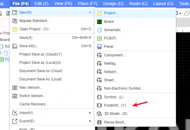
- Top Menu - File - New - footprint
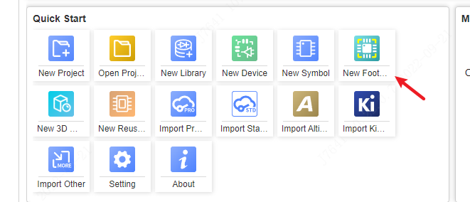
- Start Page - New Footprint
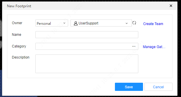
Name the footprint and choose a category.
For the footprint name naming suggestion, please refer to EasyEDA Footprint Naming Rule Reference.pdf to use scientific naming rules to facilitate management and reuse.
The corresponding footprint is drawn according to the device's data sheet.
- Download the specifications of the components to be drawn. Such as the creation of SOIC-8. eg PDF: UC2844BD1R2G
- Read the specification to obtain the footprint size and orientation information. When drawing the footprint, you need to pay attention to the 0-degree direction of the footprint (0 degree is the angle you are currently drawing, when the footprint is placed in the PCB, its angle is displayed as 0 degrees in the property panel), which is good for SMT patches. For details, please check: [PCB footprint library 0 degree graphics production standard] (http://club.szlcsc.com/article/details_12157_1.html)
- Check the footprint size, pin direction and polarity, and then place the pads on the canvas. You need to adjust the shape and size of the pad according to your actual situation.
- Component pin orientation, page 1, counts 1 to 8 counterclockwise.
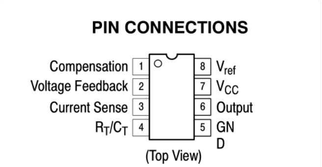
Component polarity, page 1, page 18, the orientation is horizontal.
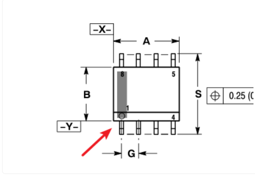
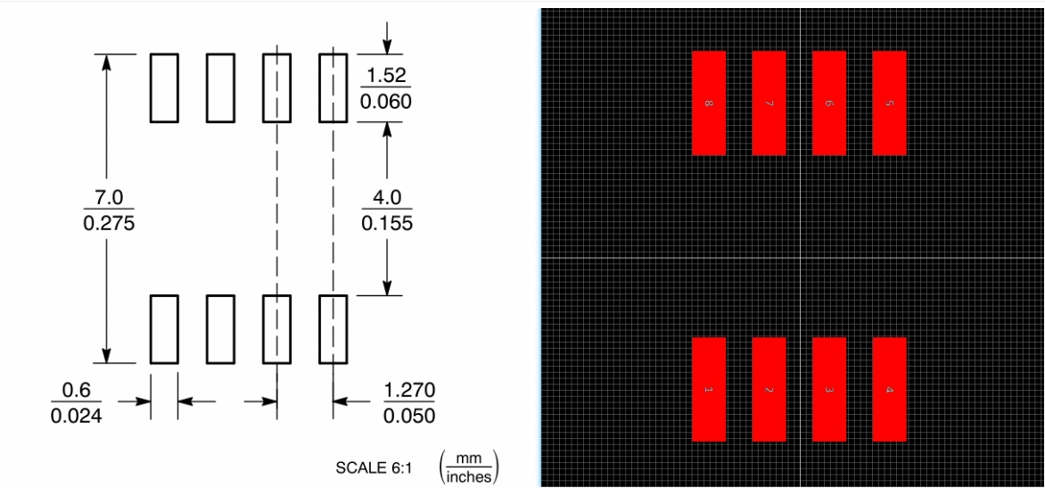
Place the pads on the top layer according to the dimension drawing on page 18 (some gold finger footprints require the top and bottom layers to be placed at the same time). Need to modify the properties of the pad, including pad number, type, size. First determine the coordinates of the first pad, and then place multiple, evenly distributed using the alignment tool on the top menu. If the moving pad step distance is not suitable, you can modify the grid size on the right.
Draw component border silkscreen. Sometimes the corresponding logo graphics can be placed on the mechanical layer and the document layer.
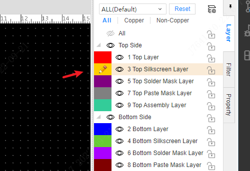
- Switch layer to top silkscreen.
- Use wire, arc and other tools to draw component silkscreen.
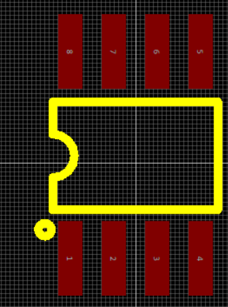
- At least one center point of the placed pad should be on the grid line as much as possible, so as to avoid the difficulty of connecting the wire to the pad when using the footprint.
- Numbers and letters can be set for the pad number, which must correspond to the pin number of the component one-to-one, otherwise the component will report an error in the footprint manager in the schematic diagram after this footprint is specified, and cannot be converted to PCB.
- Pad numbers can be incremented by mouse Place, and will remain the same if copied by pasting.
- After drawing the footprint, it is recommended to modify the coordinate origin of the footprint to the center of the footprint: it is convenient to keep the mouse in the center of the graphic when rotating; the SMT machine reduces the component adjustment work when recognizing the center of the component.
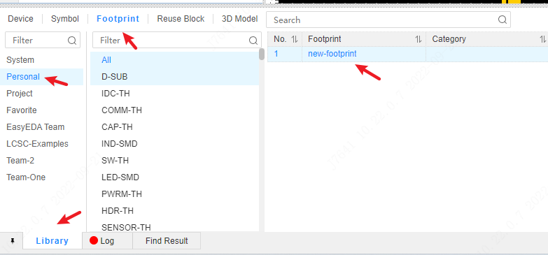
after finish, you can find it at: Bottom Panel - Library - Footprint - Personal