device
Place the device
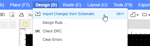
1.When the schematic diagram is transferred to the PCB, or when the PCB is imported and updated, the device will be automatically placed in the PCB.
When the schematic diagram is transferred to the PCB, the relative position of the components in the schematic diagram will be placed in the PCB by default, which is convenient for quick component layout search.
2.You can also place new components on the PCB in the bottom component library. 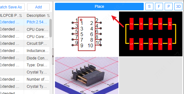
After selecting the component with the mouse, drag to place the component position.You can also use the automatic layout function of the layout menu, which is currently an experience version and is under development.
Device Properties
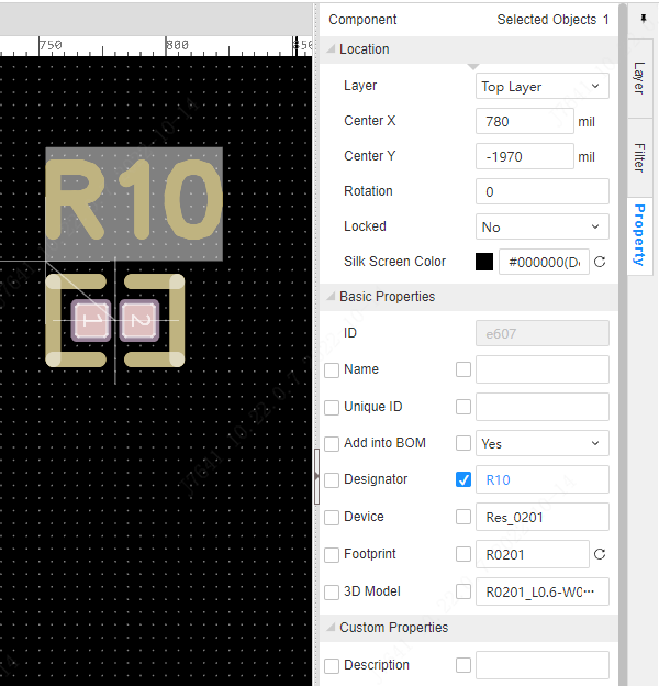
After clicking a component, you can view and modify the properties of the component in the property panel on the right
Edit Footprint
If you need to modify the pads of the package directly in the PCB, you can click the pads in the package to modify the properties (such as modifying the pad size, coordinates), and the modification will not affect other identical packages.When right-clicking to edit a mask, the mask template before modification will be opened. 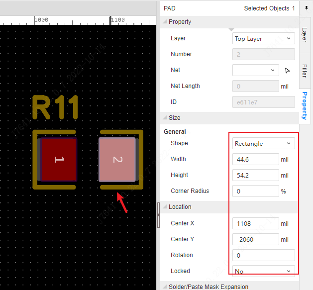
If you need to restore the original package template, after selecting the component, click the restore button icon of the package attribute in the property panel on the right to restore the modification, right-click menu to revert footprint template.
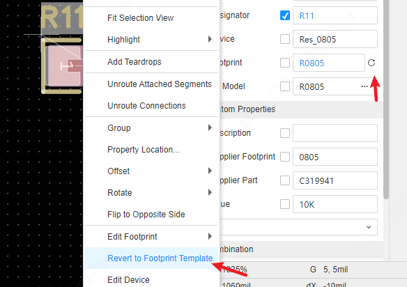
You can also right-click on the package and edit the package.This method can directly modify the project library template and support synchronous modification of the global package.Editing the package will open the package editing interface, which will be automatically synchronized to the PCB after saving.
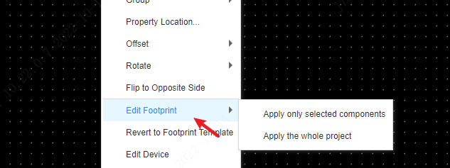
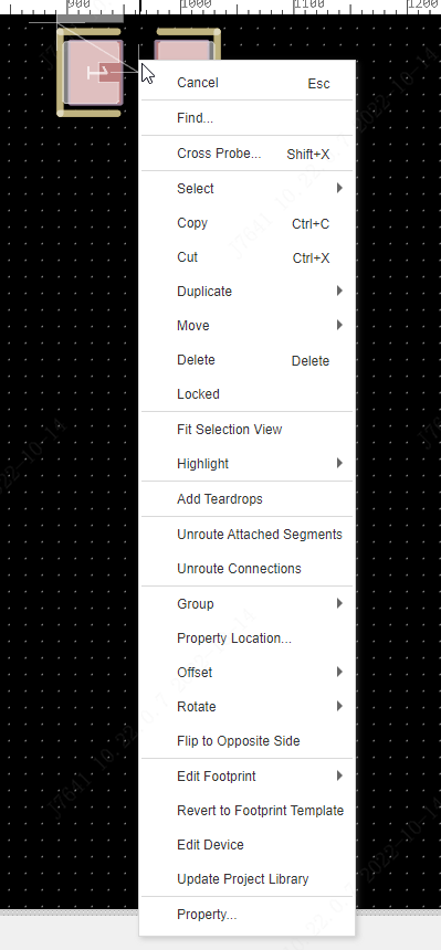
right click menu
The encapsulated right-click menu supports a lot of functions and can be used according to your own needs.