Pad
The pad is the basic unit of surface mount assembly, which is used to form the land pattern of the circuit board, that is, various combinations of pads designed for special component types.
Place pad steps:
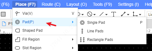
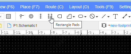
- Place using the shortcut P or the shortcut toolbar at the top.
When a pad is selected, its corresponding properties can be modified in the property panel on the right, or double-click with the left mouse button to pop up the properties dialog box to modify its properties.
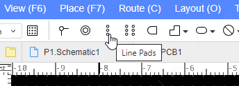
Line pads
Pad arrays are generated from the drawn bars, and pad arrays can also be generated from the values entered in the dynamic input box.
illustrate:
- Pad arrays can only be generated by drawing straight lines, not polygons.
- Does not support generating pads in multiple directions at the same time, the market is generated in one direction at a time.
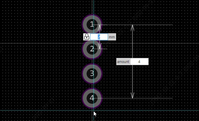
Press Tab key to change the input filed to change the parameters.
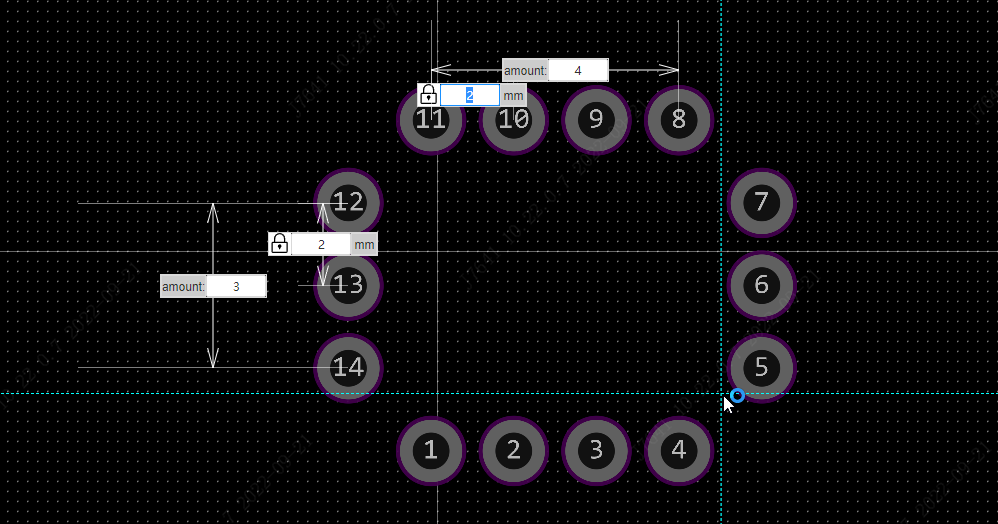
Rectangular Multipad
Generate a pad array based on the drawn rectangle, or you can generate a pad array by entering the value in the dynamic input box.
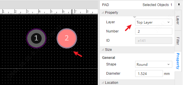
Modify the SMD pads
Select the pad and set the layer to the top or bottom layer in the property panel on the right to modify the pad into a SMD pad.