Update PCB to schematic
Under normal circumstances, PCB design needs to complete the schematic diagram first, and import the latest netlist into the PCB through the schematic to PCB or PCB import update function. After the PCB layout and routing is completed, if you need to reset the bit number based on the PCB layout information, or replace a certain component, you can complete such operations in the PCB first, and then update to the schematic in reverse. ways to improve work efficiency.
Operation entrance:
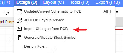
In Schematic, Top Menu - Design - Import Changes from PCB
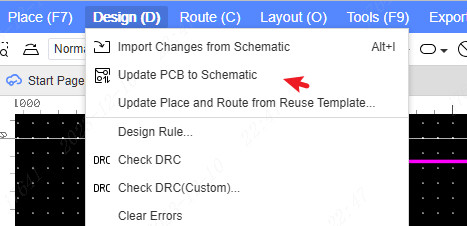
PCB, Top Menu - Design - Update PCB to Schematic
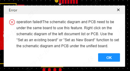
Note: When converting PCB to schematic, you need to ensure that they are under the same board, otherwise they will not be able to be converted to each other.
Check netlist differences
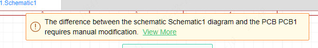
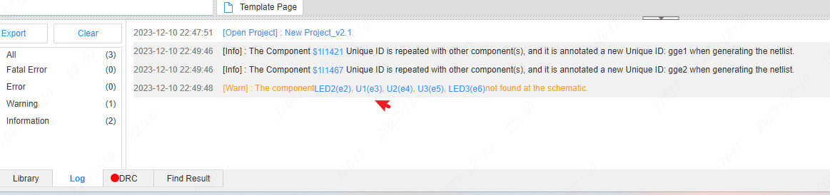
PCB to schematic diagram only supports the modification of component attributes (such as modifying the component's device and tag information). The addition, deletion of components, and network modifications will not be transferred to the schematic diagram. At this time, relevant prompt information will appear in the center of the log and canvas.
You can click on the component in the log to locate the specific location of the schematic diagram, view and make modifications.
Modifications to the component properties will appear in the pop-up confirmation import information pop-up window that pops up next.
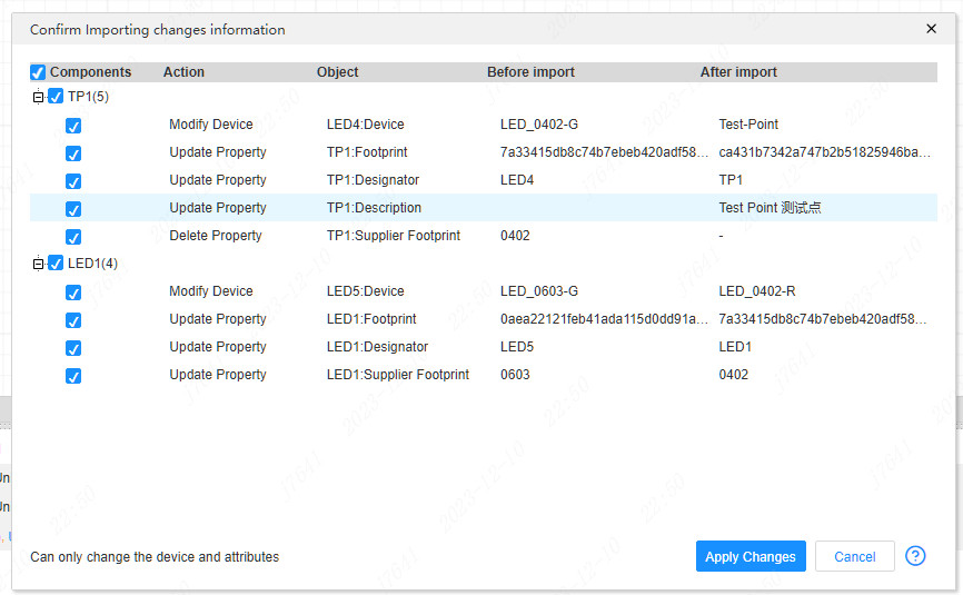
Apply changes
Check and check the items that need to be modified, click Apply modifications, and the corresponding properties will be updated to the schematic.