Import Altium Designer
EasyEDA Pro supports importing into Altium Designer.
Several versions of Altium Designer have been supported, supporting plaintext ASCII format. At present, there is a problem with importing binary format, which is not supported for the time being.
It is recommended to use EasyEDA Pro format converter for format conversion.
WARNING
- Due to the inconsistency of the format and graphic element design, there may be some differences after the graphic element is imported, please check carefully. For specific differences, please refer to the help documentation.
- EasyEDA Pro is not responsible for any losses caused by format conversion differences, if you do not agree, please do not import.
- EasyEDA Pro is compatible with the format of Altium 17. The formats of the latest or older versions of Altium may vary, and there may be differences in import. Please check carefully, and if you find any discrepancies, please contact us. We will do our best to ensure compatibility.
Import Altium project file
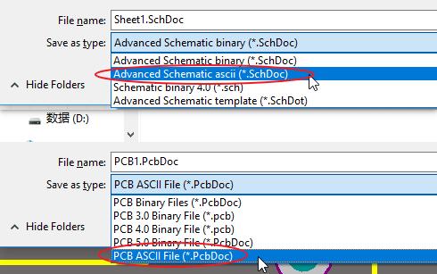
Open the schematic diagram and PCB in Altium Designer, in "File - Save As", select "altium Advanced Schematic ascii(*.SchDoc)" or "PCB ASCII File(*.PcbDoc)"
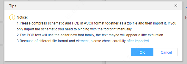
footprint the exported schematic diagram and PCB files into a compressed footprint ZIP format. Compression format only supports zip.
Note: It also supports the import of a single schematic or PCB, but the import of a single schematic cannot automatically bind the footprint, and it needs to be manually bound after import.
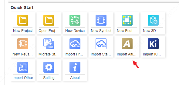
- On the professional version start page - import Altium to import.
Click OK and select the imported file.
When importing, you can choose different options according to your needs. 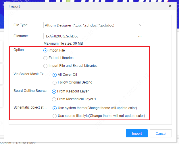
options:
- Importing files
- Extract library files
- Import files and extract libraries
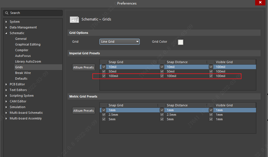
Via solder mask extension:
- All are covered with oil by default. It will force all vias to be covered with oil (solder mask extension is set to -1000)
- follow the original setting. It will be set according to the solder mask parameters of the vias in the original altium file.
Border source:
- From the Keepout layer. Many users use the keepout layer to draw borders, so this layer is used as the border by default.
- From mechanical level 1. When mechanical layer 1 is selected, the closed keepout layer will be turned into a forbidden area, and the unclosed keepout layer will be transferred to the mechanical layer.
Batch import Altium files
Please refer to the method below.
Download the AltiumScript script.
Download EasyEDA Format Converter
Or download export-altium-design.zip
After decompression, open the export-altium-to-ascii.PrjScr project in Altium Design, if the version of Altium is too low, it may not be able to run, please verify it yourself.
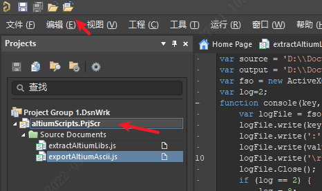
On the top menu - File or DXP - Run Script (File/DXP - Run Script) to open the script dialog box
Select the name of the script to be run, and click Run.
convertDesignToAscii.js: Convert the selected schematic and PCB files to ASCII format
convertLibToAscii.js: Convert the selected schematic library and PCB library files to ASCII format
After running the script, the script will automatically create a schematic or PCB file, and put the libraries in the currently installed library file into the document one by one. During the period, there may be multiple pop-up windows, and you need to manually click Confirm to continue.
After completion, you will find the automatically generated ASCII file in the custom output directory.
Compress the generated schematic diagram and PCB file together into a zip package and import it into EasyEDA, and choose to extract the library or import the file.
Precautions
The difference before and after format conversion is as follows:
Schematic/Component library:
| Elements/Layers | After Import | Notes |
|---|---|---|
| Bus/bus entry | Import is not supported | The bus and bus branch of the professional version are designed differently from altium and cannot be directly imported and used |
| Pictures | Import is not supported | altium pictures are stored in local file paths, and ASCII files do not contain pictures |
| Off Sheet Connector | Converted to Circular Network Identifiers | Offmap Connectors are not supported in Pro Edition |
| Sheet Symbol | Imported as hierarchical icons | Pin styles for page breaks are not supported |
| Sheet Entry | Does not support import | Professional version does not support drawing entry |
| Device Sheet symbol | Does not support import | Professional version does not support device page symbol |
| Harness | Import is not supported | Harness entities are not supported in Professional Edition |
| Directives | Some does not support import | The professional version supports No ERC labels, and does not support other indication entities (differential pairs, parameter settings, coverage areas, compilation shields) |
| Text/Text Frame/Comment | Import as normal text | The professional version does not support comments at the moment. If the corresponding font is not installed in the operating system, the default font will be used after the text is imported, and the position of the text may be slightly shifted due to different fonts; When the altium file is saved as ASCII, the Chinese may be garbled, and the garbled characters will be automatically converted to underscores after import |
| Bezier curve/ellipse arc/ellipse | Import as multi-segment polyline | Professional version does not support Bezier curve, Bezier curve, ellipse arc, ellipse |
| Component Designator | Multi-part designator as U1A, U1B after import is U1.1, U1.2 | The professional version does not support the multi-part designator method like altium |
| Pin type | Unsupported types are converted to input types | The professional version only supports three pin electrical types |
| Hidden pins | Show after import | Professional version does not support hidden pins |
| Component footprint | After importing, "original footprint 1, original footprint 2, etc." will be generated | The professional version is not associated with the footprint name, but with the uuid of the footprint, so when importing, multiple previously associated footprint names will be altiumded as common attributes |
| Theme style | The default theme of the professional version is used in the import dialog box | The default theme is that the rounded rectangle is converted to a right angle, the fill color is not preserved, and the color of the primitive is not preserved, so as to switch the schematic theme, and the theme of the original file follows the original file Style, color does not change when switching themes |
| IEEE symbols | Some IEEE symbols are not yet supported for import | The new version of altium has new IEEE symbols, some of which are not supported for import |
PCB/Footprint Library:
| Elements/Layers | After Import | Notes |
|---|---|---|
| Polygon Pour | polygon pour will be re-laid after importing | Because the polygon pour logic is different, the polygon pour filling of the PCB will also be slightly different. For example, heat welding generation method, heat welding width, whether heat welding is generated (priority will be avoided to avoid heat welding for graphics elements with wrong DRC spacing), and flying lines may be generated; horizontal and vertical polygon pour will be converted to grid polygon pour; altium polygon pour on the grid will heat and weld the vias separately, which is not supported by the professional version, and some vias may not be connected to the polygon pour after rebuilding the polygon pour (when the grid is relatively large); the professional version does not support non-signal layers polygon pour, so the polygon pour on other layers of altium will be transferred to the top layer polygon pour |
| Design Rules | Some design rules do not support import | For example, custom altiumvanced design rules, design rules not supported by the professional version, common safety spacing, etc., the parameters of the imported PCB file rules need to be altiumjusted by yourself |
| Text/Text Box | Font changes and positions will be slightly offset | If the corresponding font is not installed in the operating system and the professional version of the font setting does not altiumd the corresponding font, the text will use the default font (Arial and Times New Roman) after importing, due to the text There may be a slight offset in different positions of the font; if it is the same font, because the font display logic is different, it cannot be completely consistent with the original file, and there will be position offset and size difference; strokes and barcodes will be converted to normal text |
| Internal Electrical Layer | The network of the block may change after importing | The implementation of the internal electrical layer of altium and the professional version is different. When there are multiple internal electrical blocks, the network of the blocks may not be completely consistent, so you need to be careful Check; the internal electrical layer will rebuild the block after importing, and the internal electrical layer block division may also be different |
| keepout layer | is converted to frame layer by default | In the import pop-up window, it is supported to set whether the source of the frame is the keepout layer or the mechanical layer 1; the keepout closed lines inside some boards will automatically be converted to the corresponding forbidden area according to the target; Closed keepout primitives will be imported to the mechanical layer. The professional version does not support independent lines as forbidden areas |
| Board Shape | Go to the document layer by default | The professional version does not have a board shape but has a border layer. Since most people use keepout and mechanical layer 1 as the board frame, the board shape goes to the mechanical layer |
| Define Board Cutout | Go to the frame layer or convert to the cutout area | This function corresponds to the cutout area of the professional version |
| Polygon Pour Cutout | Convert to prohibited area | Convert to multi-layer prohibited area, the prohibited content is polygon pour |
| Mechanical Layer | Mechanical layer 1 is transferred to the mechanical layer by default, and other mechanical layers are transferred to the user-defined layer | The professional version uses the user-defined layer to realize the functions of other mechanical layers of altium |
| Ratlines | Flying lines appear after importing | It may be that the reconstruction of polygon pour after importing lealtiums to disconnection in some places, such as no network primitives, heat welding cannot be generated due to DRC spacing, etc. |
| Room | Does not support import | Professional version does not support Room primitives |
| Layer Stack Settings | Import is not currently supported | To be supported later |
| 3D Body/3D Model Library | Does not support import | The 3D binding design of the professional version is different from altium |
| Drill table | Import to Drill layer | Professional version has separate Drill layer |
| Solder Mask and Paste Mask Extension | Only pad/vias support import | Solder mask and Paste Mask extensions of other wires, arcs and other primitives do not support import. If they are independent primitives, they will be in the solder mask or solder flux layer (solder paste layer) generate an expanded primitive |
| Pad | Import to the bottom layer or top layer or multi-layer | Professional version of the pad does not support setting in any layer, the pad of the unsupported layer will be converted to the filling area of the corresponding layer; the rectangular drilling is not supported, it will be converted to Groove Drilling |
| Component/Footprint | Import to the top layer or bottom layer | If the footprint attribute drawn in altium is on the top layer, but the whole is on the bottom layer (belonging to wrong data), it will automatically correct the layer attribute to be on the bottom layer after importing; if there are multiple files with the same name but different sizes footprint, the import will take one of them as a template by default to associate with other components |
| Coordinates | Import as Text and Lines | Coordinate primitives are not supported in EasyEDA Pro |
| Dimensions | Partial support for import | Support for importing linear dimensions, angles, and dimensions, but not for partial import as text and lines |
| Object from file | Import not supported | This calls an object outside the file, not contained in the file, and does not support import |
| Work Guides | Import is not supported | This element is not supported in Professional Edition |
Other considerations:
Please do not repeatedly export your schematic or PCB to altium format and import them again, this operation may cause loss of details! ! !
When importing Altium files, if there are unsupported characters (such as garbled characters), they will be automatically converted to underscores, so after importing, you may find that there is an extra underscore in network labels, device names, footprint names, attributes, etc. Please modify it manually. When the current version of altium is saved as an ASCII file, the Chinese will become garbled, so it is also garbled when imported. You need to open the ASCII file with a text editor such as Notepad and then import it after correction.
The imported altium file supports a maximum size of 100MB. Larger files will lealtium to longer import time or import failure. It is recommended to manually reduce the file size. For example, delete the copper filling first (set the copper filling to no filling type) and then import.
Common Problem
1.Chinese garbled characters appear when importing altium schematic
In versions below altium17, the encoding of the ASCII file saved as may be GBK2312, and the encoding of the ASCII file needs to be converted from GBK2312 to UTF-8. You can save as a UTF-8 encoded file using a text editor.
method:
- Save as ASCII file with altium17, which defaults to UTF-8 encoding
- Or open the ASCII file with the system's Notepad, and select UTF-8 encoding when saving as. Other text editors also have corresponding encoding conversion functions.
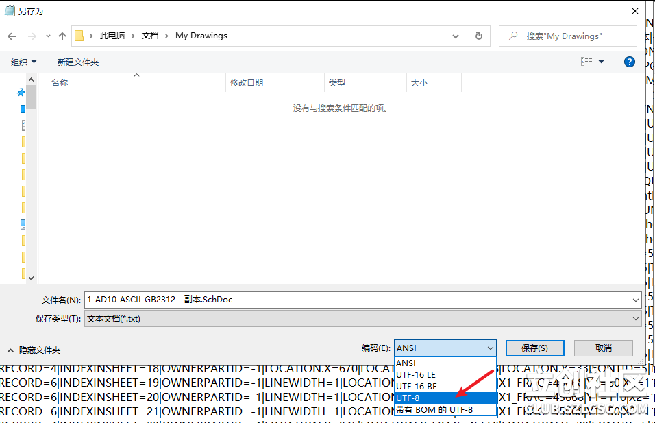
If after the text encoding is converted to UTF-8, there are still garbled characters when viewing the content with a text editor, then the import will also be garbled characters, please correct it in the text editor before importing.
2.After importing the altium file, there are wires and device pins that are not aligned with the grid, or the pins are biased
First set the unit of the schematic diagram in Altium Designer to imperial mil, in: view menu - switch unit
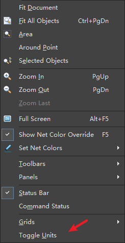
Then the canvas right-click menu or system settings: Options - Grid - set the display grid, electrical grid, altiumsorption grid to 100mil, switch grid to 100mil
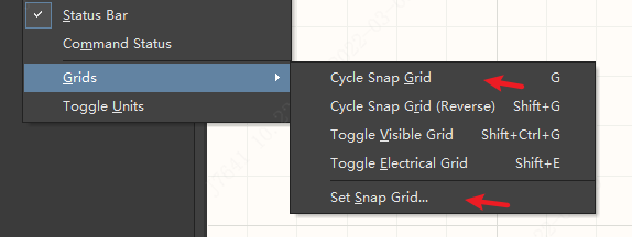
Select all schematics CTRL + A , use Edit menu: Edit - Align - Snap to Grid function. Check for broken or wrong places to correct.
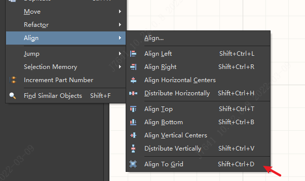
Save as ASCII and import
3.The footprint size will change after importing.
This is because the imported PCB has a footprint with the same name, but the footprint size is different. When importing, the bottom log will prompt that the footprint has the same name, and only one of them will be imported as a template.
Solution: It is recommended to manually modify the footprint names with the same name and different sizes in altium to ensure that the footprint names are not repeated.
Differences Before and After Import
Support for Format Conversion Primitives
Schematic/Component Library
Supported Primitive Types:
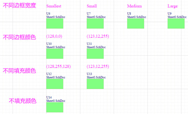
| AD Element | After Import | AD Element Style | Converted Primitive Style | Description |
|---|---|---|---|---|
| Bus | Bus | 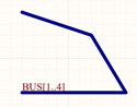 | 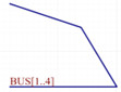 | - |
| Bus Entry | Bus Entry |  | 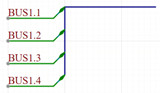 | Suspended Bus Entry is not supported during import. |
| Device | Symbol |  |  | - |
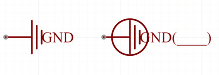
| Power Port | Network Identifier | 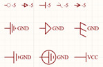 | 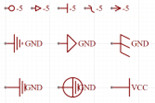 | - |
| Wire | Wire |  |  | - |
| Net Tag | Net Tag |  | 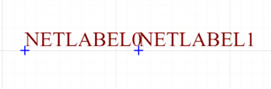 | The network label connection point in AD is light gray, and it becomes a blue cross after conversion. |
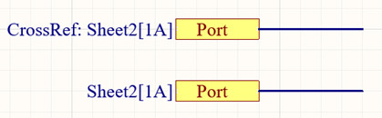
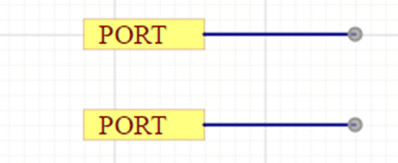
| Port | Network Port | 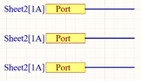 | 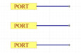 | - |
| Off-Graph Connector | Network Identity | 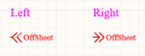 | 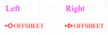 | The professional version does not support off-graph connectors. After import, the network ID is converted to a circle or triangle. |
| Page Character/Drawing Entry | Module Symbol/Pin |  |  | The professional version does not support drawing entries. They are converted to pins after import. |
| Text String | Text |  |  | - |
| Text Box/Comment | Text |  |  | Text boxes and comments are not supported in EasyEDA Pro. They are converted to text after import. |
| Drawing Tool - Arc | Arc |  |  | - |
| Drawing Tool - Circle | Circle |  |  | - |
| Drawing Tool - Elliptical Arc | Polyline | 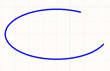 |  | The professional version does not support elliptical arcs. After import, they are converted into multi-segment polylines. |
| Drawing Tool - Line | Polyline |  |  | - |
| Drawing Tool - Rectangle | Rectangle |  |  | Professional rectangles do not support transparent operations yet. |
| Drawing Tool - Rounded Rectangle | Rectangle |  |  | - |
| Drawing Tool - Polygon | Polyline |  |  | - |
| Plotting Tool - Bezier Curve | Bezier Curve |  |  | Continuous multi-stage Bezier curves are converted into multi-segment Bezier curves after import. |
| Indication - Generic No ERC Label | No Connection Identifier |  |  | - |
| IEEE Symbol | Polyline, Arc, Circle |  |  | After conversion, it is presented as a composite element composed of multi-segment polylines, arcs, and circles. |
| Manual Contact | Node |  |  | A suspended manual contact cannot be imported. A manual contact placed on a wire is converted to a node. |
| Theme Styles | Theme Styles | - | - | By default, the import dialog box uses the default theme of EasyEDA Pro. Rounded rectangles are converted to right angles, fill colors are not retained, and pixel colors are not retained to switch the schematic theme. If the original file theme is used, the color will follow the original file style, and the color will not change when switching themes. |
Unsupported Primitive Types:
| AD Graphic Element | Graphic Element Description | Description |
|---|---|---|
| Harness | Includes signal harness, harness connector, harness entry, predefined harness connector. | Schematic design does not support wire harness elements. |
| Indicators | Including the universal No ERC label, differential pairs, parameter settings, covering regions, compilation masks, probes (present in earlier versions). | The current schematic design supports only the conversion of the universal No ERC label connected to the device pin. The remaining indicators do not support conversion at this time. |
| Image | Image. | Altium Designer stores images in a local file path that does not contain images. |
| Hidden Pins | Hidden pins in the device. | EasyEDA Pro does not support hidden pins, which will be displayed after import. |
| Device Page Characters | - | EasyEDA Pro does not support device page characters. |
Primitive Differences:
Text String Conversion Differences:
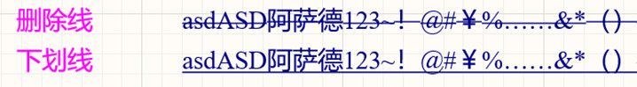
- The strikethrough effect is lost after conversion.EasyEDA Pro text-related symbols do not support strikethrough effects, so all text-related symbol strikethrough effects will be lost.
- The underline display effect is slightly different. The underline of text primitives in the EDA Professional edition is thicker than that in Altium Designer and will not cover the character content.
- The locking information effect is lost. Since the symbol elements of the EasyEDA Pro do not support locking, all locking effects of elements with locking will be lost.
- Font differences: If the operating system does not have the corresponding font installed, the text will be imported using the default font, and the text position may shift.
- If the AD file is saved as ASCII, Chinese characters may become garbled. After the AD file is imported, the garbled characters are automatically converted to underscores (-).
Altium Designer 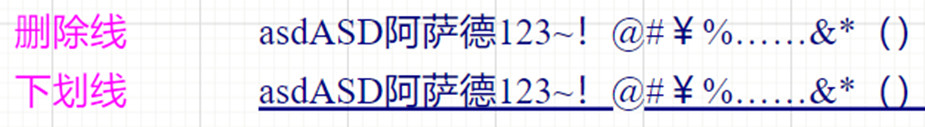
Strikethrough and Underline Effect
Bus Conversion Differences:
- The line width of the bus is significantly reduced after conversion. This issue will be addressed in a future version.
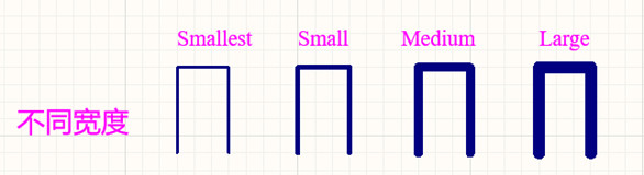
Altium Designer Bus with Different Line Widths 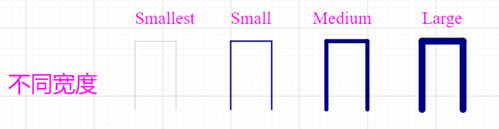
Bus Entry Conversion Differences:
- The style of bus entry primitives is different after conversion.
- The color of bus entry is different after conversion. Altium Designer allows the color of bus entry elements to be revised, but this operation is not supported by the EDA Professional Edition at present. The color of bus entry is green after conversion.
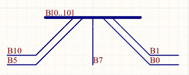
Bus Entry in Altium Designer 
Bus Entry
Device Component Conversion Differences:
- The device is composed of multiple symbolic primitives, and any difference in symbolic primitives may cause conversion differences in the device.
- There are differences in pin color. The pin color is the default color after import.
- Pin electrical type import is not supported and will be lost after conversion.
- When the custom attribute in the Altium Designer element is the same as the system attribute, the system attribute will be overwritten by the custom attribute after conversion.
- The connection point style is different after conversion.
- "Original package 1, original package 2, etc." will be generated after the component package is imported. The professional version is not associated with the package name but according to the package UUID. Therefore, the original associated multiple package names will be added as ordinary attributes when importing.
- Component bit numbers: The professional version does not support the AD multi-component bit number method. Multi-component bit numbers such as U1A, U1B will be converted to U1.1, U1.2 after import.
Power Port Conversion Differences:
- The EDA Professional network name only supports uppercase English letters and some common characters. If the network name contains Chinese, lowercase English letters, Greek letters, or other special characters, lowercase English letters will be converted to uppercase, and Chinese and special characters will be converted to underscores "_".
- There is a difference in the style of the Power port between GOST Power Ground and GOST Earth, which will be addressed in future versions.
- There is an offset in the position of the Power port names for GOST Power Ground and GOST Earth, which will be fixed in a future release.
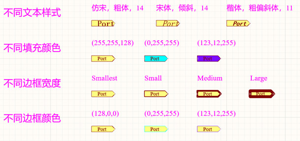
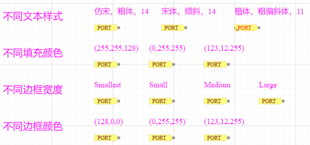
Port Conversion Differences:
- The name and value information of Port properties are lost after conversion. The EasyEDA Pro network port does not currently support property information.
- The EasyEDA Pro network port does not support revising font, border width, border color, and fill color. Such information will differ after conversion.
- The I/O attribute of the Port is lost after conversion.
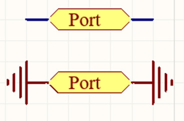
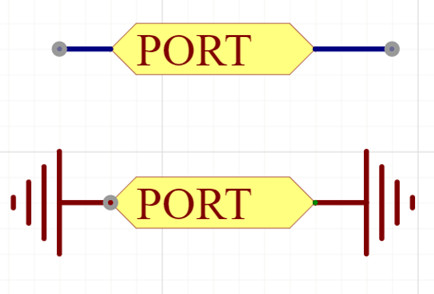
- If the Port in Altium Designer is connected to an unnamed wire or bus, the Port name is assigned to the wire or bus after conversion.
- If both ends of the Port in Altium Designer are connected to a wire, both ends remain connected to a wire after conversion. If both ends are connected to a network ID, only one end with a pin can be connected after conversion.
Page Character Conversion Differences:
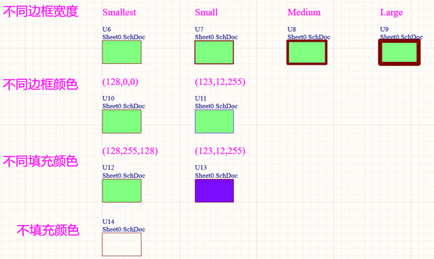
- After the page character is imported, it will be presented as a module symbol. The EasyEDA Pro does not support revising the border of the module symbol, whether to fill, fill color, and lock operations. Therefore, there will be differences in the fill, border, and lock status after conversion.
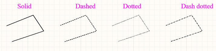
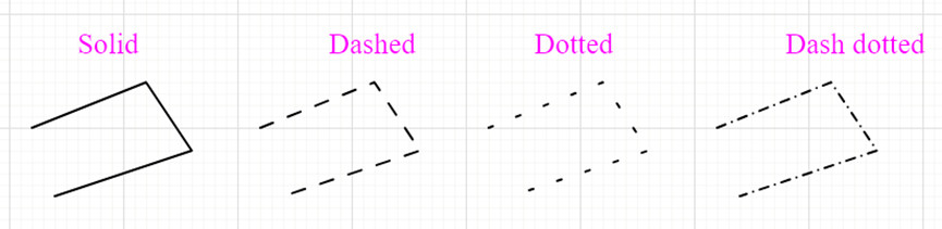
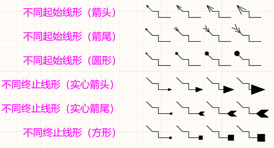
Line Conversion Differences:
- There is a difference in line style after conversion.
- The Start Line Shape and End Line Shape in Altium Designer are not supported in the EDA Professional Edition, so they will be converted to multiple polylines.
PCB/Package Library:
Supported Primitive Types:
| AD Element | After Import | AD Element Style | Converted Primitive Style | Description |
|---|---|---|---|---|
| Device | Component | 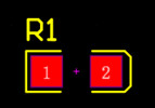 |  | - |
| 3D Component Body | Contour Object |  |  | The professional version does not support importing 3D components. It is converted to a line or fill region depending on the layer it is on. |
| Fill | Fill Region |  |  | - |
| Solid Region | Fill Region |  |  | - |
| Arc | Line - Two Points Arc |  |  | - |
| Circle | Line - Circle |  |  | - |
| Line | Wire | 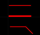 | 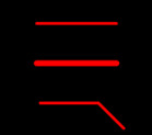 | - |
| String | Text | 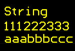 |  | For now, only the first line of text will be imported; this will be supported in future versions. |
| Pad | Pad |  |  | - |
| Via | Via |  |  | - |
| Trace | Lead |  |  | - |
| Rectangle | Line |  |  | - |
| Graph | Contour Object |  |  | The kind set as polygon cut will be converted to a prohibited copper region. |
| Keepout | Board Frame |  |  | The default value is the board frame. |
| Copper | Copper Region |  |  | - |
| Polygon Copper Hollowing | No Region - No Copper Region |  |  | - |
| Drilling Table | Text, Lines |  |  | Converted to text and line composite primitives. The layer is converted to the drill layer. |
| Cascade Structure Table | Text, Line | 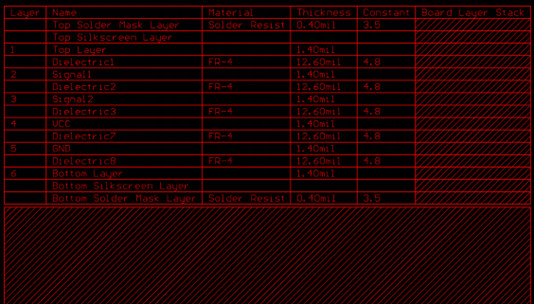 | 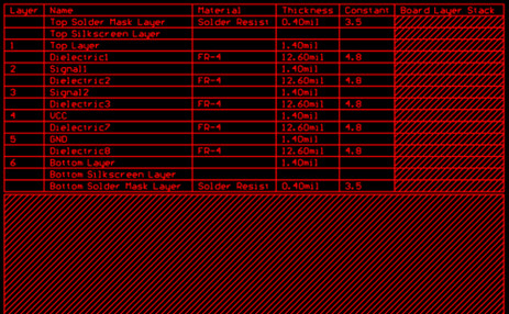 | Converted to composite primitives of text and lines. |
| Size | Size |  |  | The size styles are different. Some dimension layers are converted to document layers. |
| Teardrop | Teardrop |  |  | - |
Some Layers/Features:
| AD Layer/Function | After Import | Description |
|---|---|---|
| Board Shape | To the Document Layer by Default | EasyEDA Pro does not have a board shape but has a border layer. Most users use the Keepout and Mechanical Layer 1 as the board frame. Therefore, the board shape is converted to the mechanical layer. |
| Internal Electrical Layer | Block Network May Change After Import | The implementation of the internal electrical layer differs between AD and the professional version. When there are multiple internal electrical blocks, the block network may not be entirely consistent and needs to be carefully checked. After importing, the inner electrical layer will reconstruct the block, and the division of the inner electrical layer block may also differ. |
| KeepOut Layer | Default Plate Frame Layer | In the import window, you can set the source of the plate frame to be the Keepout layer or Mechanical Layer 1. Closed Keepout lines inside some boards are automatically converted to the corresponding prohibited region according to the action object. Open Keepout elements are imported into the mechanical layer. The Pro version does not support independent lines as prohibited regions. |
| Mechanical Layer | Mechanical Layer 1 to the Mechanical Layer, Other Mechanical Layers to the User-Defined Layer | The professional version uses the user-defined layer to implement the functionality of the other mechanical layers of AD. |
| Flying Lines | Flying Lines Appear After Import | Some places may be disconnected due to the reconstruction of copper after import, such as the absence of network elements, thermal welding not being generated due to DRC spacing, etc. |
| Element Solder Mask Extension | Only Through-Hole of Pad Supports Import | Other wire, arc, and other elements' solder mask extensions are not supported for import. In the case of independent primitives, an extended primitive will be generated in the solder mask or aid layer (solder paste layer). |
| Define Board Cutout | To the Border Layer or to the Grooving Region | This function corresponds to the grooving region of the professional version. |
Unsupported Primitive Types:
| AD Element | Description |
|---|---|
| Design View | The working view is not supported in EasyEDA Pro. |
| Work Wizard | This primitive is not supported in EasyEDA Pro. |
| Objects from a File | Such objects that call outside the file, are not contained in the file, and are not imported. |
| 3D Volume | The Pro edition does not support 3D volume primitives. |
| Mosaic Array | Implementation logic is different; import is not supported. |
| Coordinates | EasyEDA Pro does not support coordinate primitives. |
| Room | Room primitives are not supported in EasyEDA Pro. |
Primitive Differences:
Device Conversion Differences:
The device is composed of multiple package elements, and any package element difference may cause the conversion difference of the device.
If there are multiple packages with the same name but different sizes, the import will default to using one of them as a template to associate with other components.
There may be differences in the encapsulation layer after conversion:
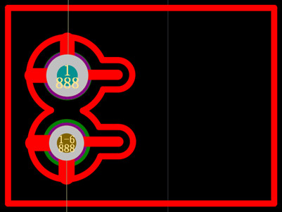
A. The layer property of the component in the professional version only supports the top or bottom layer. The layer property of the component is changed to the top layer after the conversion of other layer devices, but the pixel in the device is still in the corresponding layer.
      <div align="center">
      <img src="/storage/images/cn/import-export/import-altium-designer/import-altium-designer_20241010_190740.jpg" style="max-width: 60%;">
      <figcaption style="text-align: center; font-size: smaller;">Different layers of devices in Altium Designer</figcaption>
      </div>
      <div align="center">
      <img src="/storage/images/cn/import-export/import-altium-designer/import-altium-designer_20241010_190817.jpg" style="max-width: 60%;">
      <figcaption style="text-align: center; font-size: smaller;"></figcaption>
      </div>
B. If the encapsulated attribute drawn in AD is at the top level, but the whole is at the bottom level (belonging to the error data), the layer attribute will be automatically corrected to the bottom level after import.
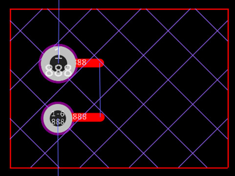
For example, the internal element of the device is transformed at the bottom level, but the package properties are transformed at the top level.
        <div style="display: flex; justify-content: center;">
        <figure style="margin: 0 10px;">
        <img src="/storage/images/cn/import-export/import-altium-designer/import-altium-designer_20241010_191003.jpg" style="max-width: 95%; display: block; margin: 0 auto;">
        <figcaption style="text-align: center; font-size: smaller;">Altium Designer device properties at the top</figcaption>
        </figure>
        <figure style="margin: 0 10px;">
        <img src="/storage/images/cn/import-export/import-altium-designer/import-altium-designer_20241010_191026.jpg" style="max-width: 100%; display: block; margin: 0 auto;">
        <figcaption style="text-align: center; font-size: smaller;"></figcaption>
        </figure>
        </div>
Text/Text Box Conversion Differences:
If the font is not installed in the operating system or the font is not added in the Pro font settings, the default font (Arial and Song) will be used after the text import, and the text position may be offset.
Due to different font display logic, the same text font may not be exactly the same as the source file, and there may be differences in position and size.
The default font of Altium Designer is converted to the Default 2 font. Chinese characters that are not supported by the default font of Altium Designer will be displayed normally after conversion, and the font will be changed to typeface.
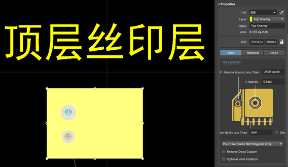
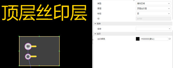
Text set in the solder paste layer in Altium Designer will become a mechanical layer after import.
The text box is converted to normal text, and only the first line of the text box is kept.
          <div style="display: flex; justify-content: center;">
          <figure style="margin: 0 10px;">
          <img src="/storage/images/cn/import-export/import-altium-designer/import-altium-designer_20241010_191623.jpg" style="max-width: 100%; display: block; margin: 0 auto;">
          <figcaption style="text-align: center; font-size: smaller;">Altium Designer text box for multi-line text</figcaption>
          </figure>
          <figure style="margin: 0 10px;">
          <img src="/storage/images/cn/import-export/import-altium-designer/import-altium-designer_20241010_191651.jpg" style="max-width: 93%; display: block; margin: 0 auto;">
          <figcaption style="text-align: center; font-size: smaller;">Keep only the first line</figcaption>
          </figure>
          </div>
Strokes and barcodes are converted to normal text. Pad Conversion Differences:
Rectangular drilling is not supported. Instead, slot drilling is used.
          <div style="display: flex; justify-content: center;">
          <figure style="margin: 0 10px;">
          <img src="/storage/images/cn/import-export/import-altium-designer/import-altium-designer_20241010_191942.jpg" style="max-width: 60%; display: block; margin: 0 auto;">
          <figcaption style="text-align: center; font-size: smaller;">Altium Designer Rectangular Bore</figcaption>
          </figure>
          <figure style="margin: 0 10px;">
          <img src="/storage/images/cn/import-export/import-altium-designer/import-altium-designer_20241010_192008.jpg" style="max-width: 48%; display: block; margin: 0 auto;">
          <figcaption style="text-align: center; font-size: smaller;">The format is converted to an oblong circle</figcaption>
          </figure>
          </div>
The electrical type attribute value will be lost after conversion.
The Professional pad does not support any layer. Unsupported layers will be converted to the corresponding fill region.
          <div style="display: flex; justify-content: center;">
          <figure style="margin: 0 10px;">
          <img src="/storage/images/cn/import-export/import-altium-designer/import-altium-designer_20241010_192331.jpg" style="max-width: 100%; display: block; margin: 0 auto;">
          <figcaption style="text-align: center; font-size: smaller;">Altium Designer Inner Signal1 Pad</figcaption>
          </figure>
          <figure style="margin: 0 10px;">
          <img src="/storage/images/cn/import-export/import-altium-designer/import-altium-designer_20241010_192401.jpg" style="max-width: 92%; display: block; margin: 0 auto;">
          <figcaption style="text-align: center; font-size: smaller;">Format Converted to Fill Region</figcaption>
          </figure>
          </div>
Hole Conversion Differences:
- The EDA Professional edition does not support setting different outer diameters in different layers. After conversion, the top layer data is used as the outer diameter of the hole.
Paving Copper Conversion Differences:
- The contour fill style of copper paving is not supported for import and is converted to a prohibited region.
- Non-copper layers and multi-layer copper are not supported for import and are converted to fill regions or other formats.
- There may be differences in re-copper placement after import due to different copper placement logic.
- Since the Pro edition does not fully support the AD ply fill style, there may be differences in the ply fill style attributes after import.
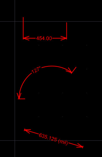
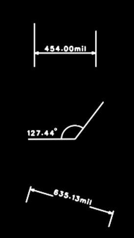
Size Conversion Differences:
- Radial, reference, lead, center, baseline, and diameter dimensions are not supported for import.
- Dimensions of non-mechanical layers and screen layers will be converted to the document layer after import.
- Dimensions and linear dimensions are converted to length dimensions after import.
- There is a difference in the converted size style due to the difference between the Pro and Altium Designer size styles.
Design Rule Conversion Support:
| Design Rules in AD | Import Corresponding Design Rules | Description | |
|---|---|---|---|
| Electrical | Clearance | Spacing - Safe Spacing | |
| Routing | Width | Physics - Wire | Extreme |
| Routing Via Style | Physical - Vias Size | ||
| Differential Pairs Routing | Physical - Difference Pair | Extreme | |
| Mask | Solder Mask Expansion | Expansion - Solder Mask Expansion | |
| Paste Mask Expansion | Extension - Weld Extension | Get SMD Pad Data | |
| Plane | Power Plane Connect Style | Plane - Inner Electrical Layer | |
| Polygon Connect Style | Flat - Copper Laying | ||
| Manufacturing | Board Outline Clearance | Spacing - Safe Spacing | Board Frame Safe Spacing |
Clearance
Safe Spacing (Simple) Conversion Table:
| Altium Designer Element | Corresponding Professional Layout Element |
|---|---|
| Track | Wire |
| SMD Pad | Patch Pad, Single-Layer Test Point |
| TH Pad | Plug-In Pad, Multi-Layer Test Point |
| Via | Via |
| Copper | Fill Region/Teardrop, Line |
| Text | Text/Image |
| - | Drill a Hole |
Safe Spacing (Advanced) Conversion Table:
| Altium Designer Element | Corresponding Professional Layout Element |
|---|---|
| Arc | - |
| Track | Wire |
| SMD Pad | Patch Pad |
| TH Pad | Plug-In Pad |
| Via | Via |
| Fill | - |
| Poly | Line |
| Region | Fill Region/Teardrop |
| Text | Text/Image |
| - | Drill a Hole |
Other Considerations:
- Please do not repeatedly export your schematic or PCB to AD format and then import it again, as this operation may lead to loss of details.
- When importing an Altium file, unsupported characters (such as garbled characters) are automatically converted to underscores. Therefore, underscores may be found in network labels, device names, package names, and attributes. These should be manually revised. When the current version of AD is saved as an ASCII file, Chinese characters may become garbled, so they will also be garbled when importing. You need to open the ASCII file with a text editor like Notepad and modify it before importing.
- The maximum size of the imported AD file is 1GB. If the file size is larger, the import will take longer or may fail. It is recommended to reduce the file size manually. For example, delete the copper filling (set the copper filling type) before importing.