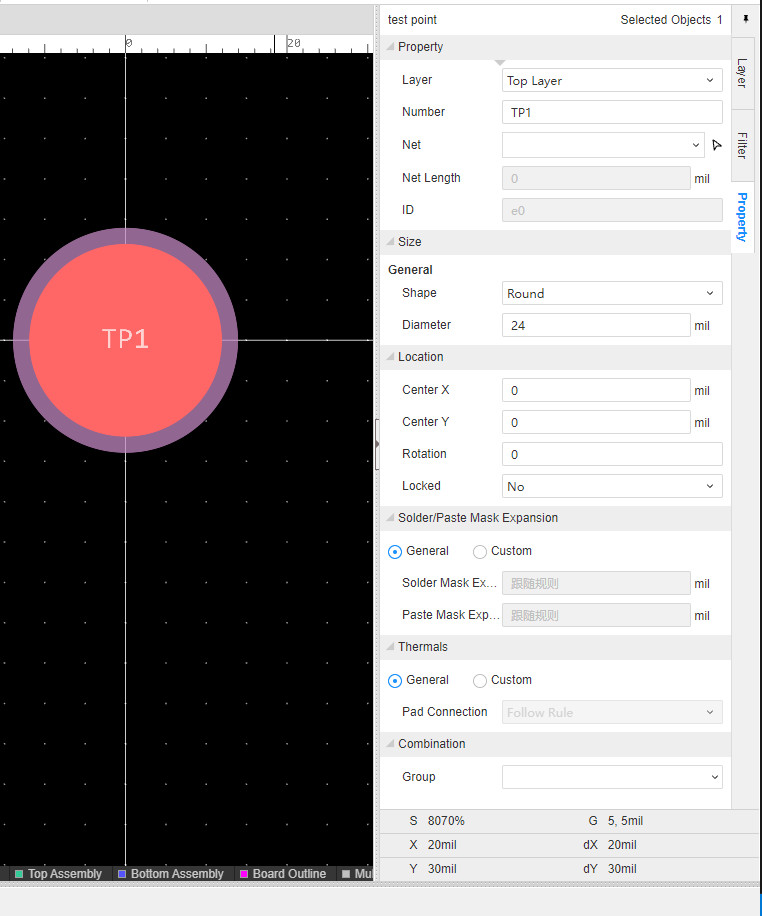
Test Point
EDA Pro supports placing test points directly on the PCB for connecting test instruments for circuit testing and fault diagnosis. Test points are usually located at critical locations on the circuit board, such as connectors, chip pins, critical signal lines, etc.
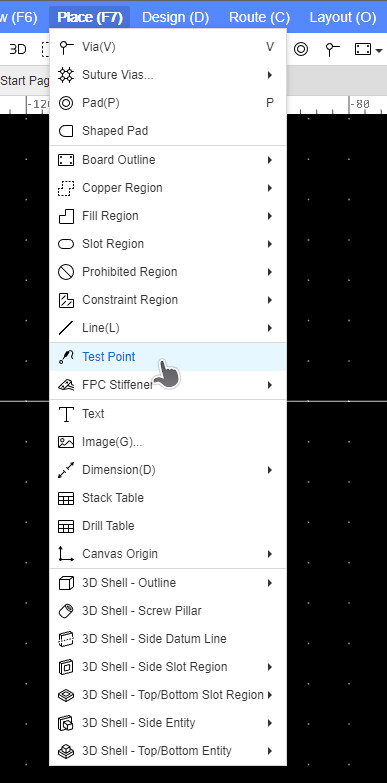
Place method:
- Top Menu - Place - Test Point,
After placement, you can set parameters such as layer, network, size and shape of the test point in the right property panel