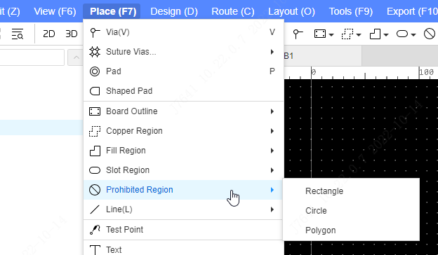
Prohibited Region
In designing a PCB, some circuits are sensitive to signals, and the signals are easily interfered. Usually, a prohibited region is set up. The prohibited region includes forbidden wiring, copper coating, and devices.
Steps:
- Top Menu - Place - Prohibited region - Rectangle
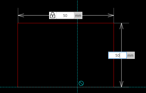
After the cross cursor appears, you can draw a rectangular prohibited region in the PCB, or you can enter the size value to be drawn in the dynamic input box
After drawing, the property pop-up window will pop up, where you can set the property of the prohibited region.
prohibited option
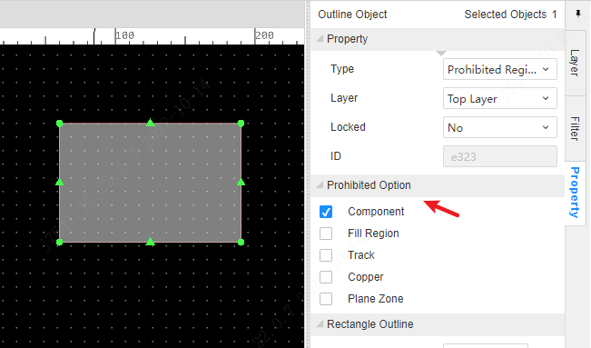
- Component: When checked, the currently drawn prohibited region cannot place components in it.
- Fill region: When checked, the currently drawn prohibited region cannot draw filled regions inside, nor can it be drawn into the prohibited region from outside. This option only for DRC checking, it doesn't like the copper option to cutout the fill region.
- Track: When checked, the currently drawn prohibited region cannot draw track inside
- Copper: After checking, the currently drawn prohibited region cannot draw the copper region in it, and the global copper-laying will cut the copper skin of the prohibited region.
- Plane Zone: After checking, the plane zone will be coutout the copper.