footprint Manager
footprint manager
Modify the footprint in batches. If there are many devices in the same footprint in the schematic, then modifying the footprint in batches will greatly reduce your workload.
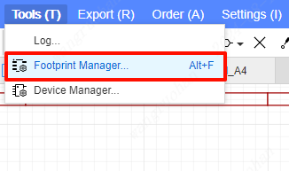
Open the footprint manager in the schematic interface, the top menu - tools - footprint manager
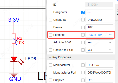
Or, upon selecting the component, click on the packaging attribute input box in the right property panel.
After opening, you can see the symbols and footprints of all devices under the project. The upper side is the symbol, and the lower side is the footprint.
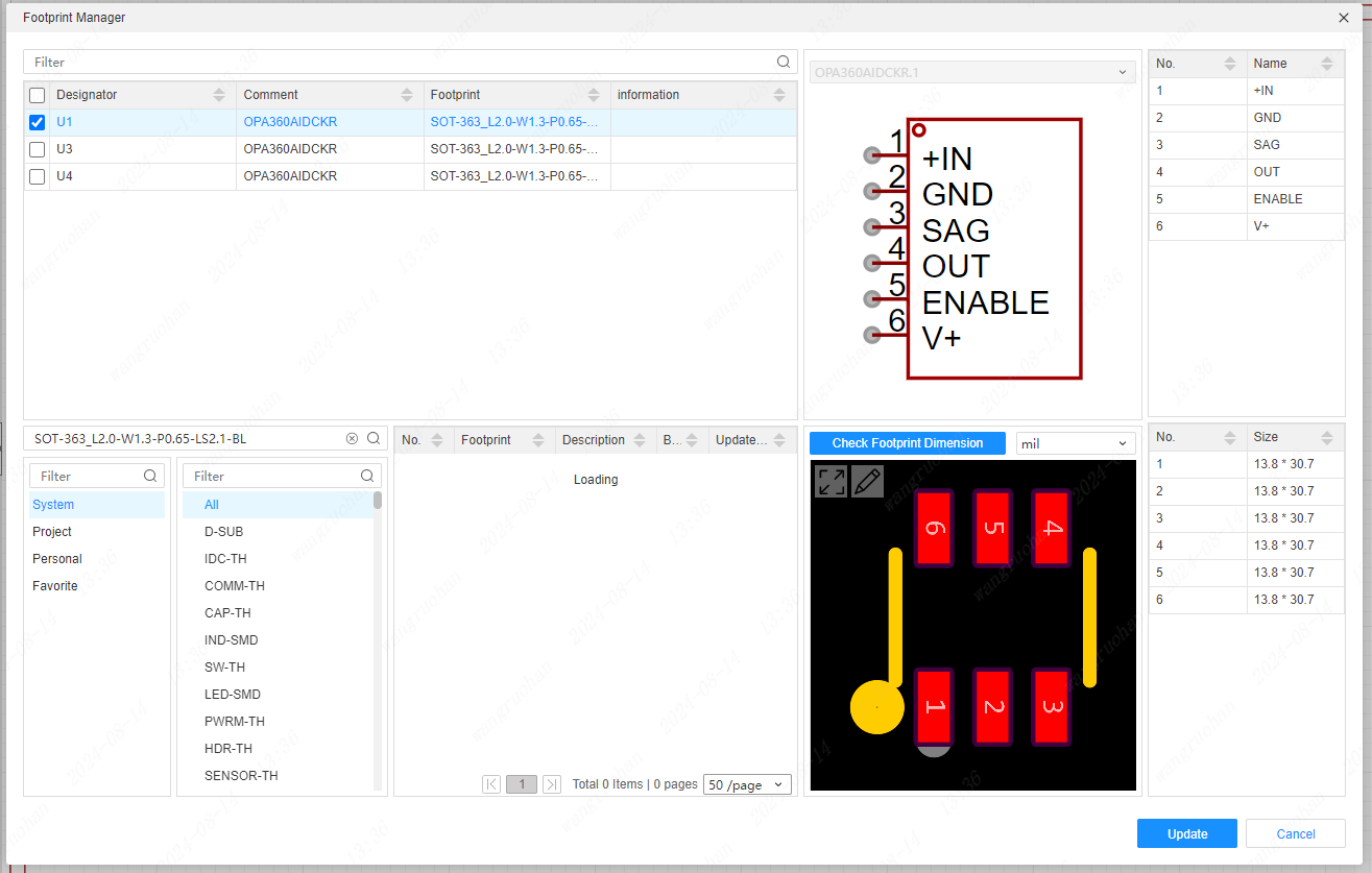
When conducting a full-screen preview of the packaging and inspecting the dimensions:
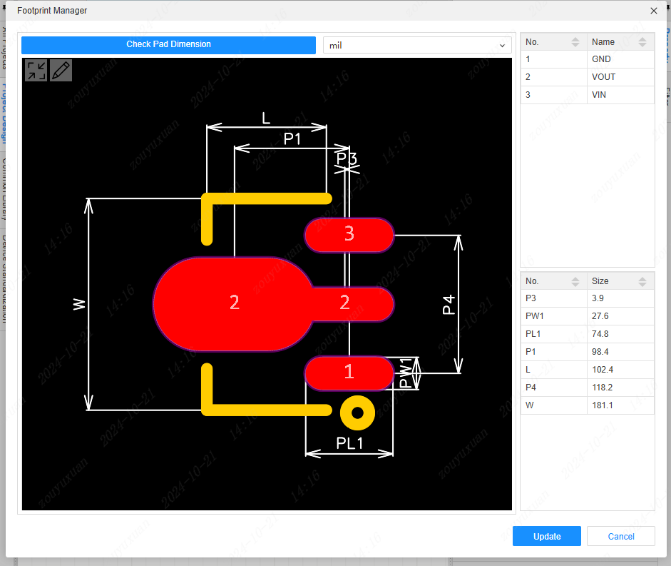
Select the device to be modified and click Update to update the latest footprint to the entire project.

When the update is complete, a prompt will appear at the top.
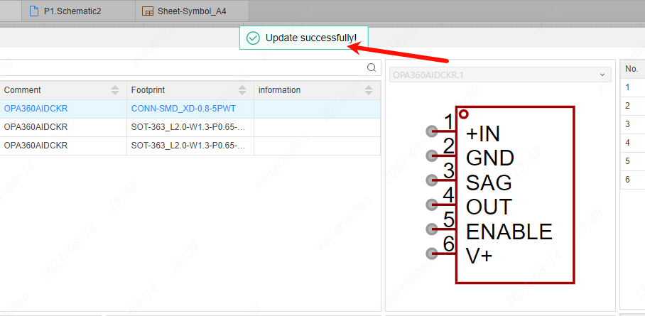
Notice:
When a component is not encapsulated, or the pin numbers of the symbol and the pad numbers of the package do not match, the information column of the component list will report an error and list the error information. The pin numbers of the components must all match the pad numbers of the package; otherwise, it is impossible to transfer to the PCB or update the PCB. The number of pins can be fewer than the number of pads.
Tips:
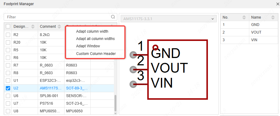
The table header of the component list supports the adjustment of column width through right-click and the customization of the table header.
