Export Altium Designer
Disclaimer
Because the format design and graphics elements are different, the exported Altium Designer files cannot be guaranteed to be completely consistent (especially the text size and position). Please be sure to check carefully after opening Altium Designer, and do not place an order without checking. EasyEDA is not responsible for any problems or losses caused by differences in the export.
If you check the exported file and the original design is very different, please contact us, we will try our best to correct it.
export project
EasyEDA supports exporting Altium Designer files in ASCII 5.0 format.
Entry: Top Menu - File - Export - Altium Designer. Or: Top Menu - Export - Altium Designer
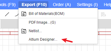
The file format of Altium Designer will be exported based on all documents of the current project and footprintd in a compressed footprint.
Known issues:
The image of the schematic diagram does not support export.
The image of PCB does not support export.
The rules of PCB do not support exporting.
The copper filling of the PCB does not support export. After exporting, you need to manually rebuild all the copper in Altium Designer.
The export of the inner electrical layer area of the PCB cannot be completely consistent, and it needs to be manually adjusted and reconstructed.
Some layers of the PCB cannot accurately find the corresponding layer of Altium, and will be exported in more mechanical layers.
Export library file
EasyEDA Pro support direct export to Altium Designer format from symbol library and footprint library. Or you can export by exporting the project.
Method 1:
Edit the symbol or footprint graphic
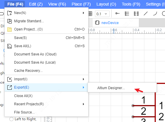
Export as Altium file via: Top Menu - File - Export - Altium Designer
Method 2:
Create a new project
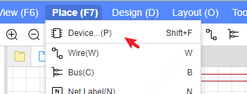
Find the corresponding device according to the library name or product number you want to export, and place it on the schematic or PCB. Shortcut SHIFT + F, or bottom bank, shortcut S.
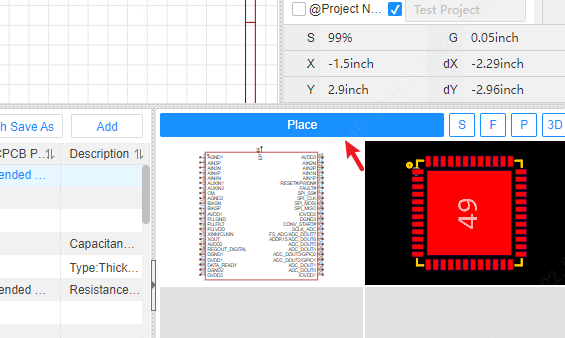
After placing the device on the schematic and PCB, save it. Export menu at the top - export Altium Designer.
Export the Alitum Designer zip footprint will contain the schematic and PCB, and open it in Altium Designer after decompression.
After Altium Designer opens the schematic diagram or PCB, go to: Top Menu - Design - Extract Library File to complete the library extraction.
Notes of Caution
Export the supported graphic elements of Altium Designer
1. Schematic Diagram
1.1. Supported Graphic Element Situations
| Professional Layout Elements | Exported Elements | Professional Layout Element Styles | Exported Element Styles | Descriptions |
|---|---|---|---|---|
| Component | Device | 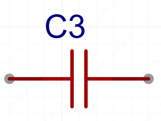 | 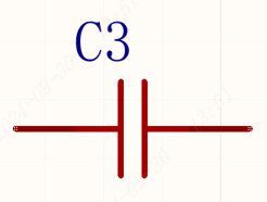 | - |
| Conductor | Line | 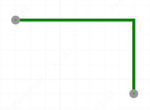 | 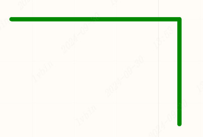 | - |
| Bus | Bus |  |  | - |
| Network Label | Network Label | 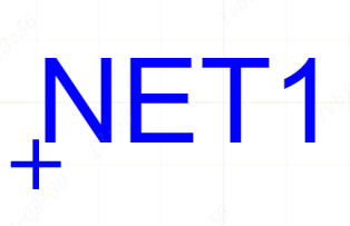 |  | - |
| Network Identifier | Power Port | 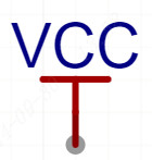 | 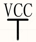 | - |
| Network Port | Port |  |  | - |
| Non-Connected Identifier | Indication - General No ERC Label | 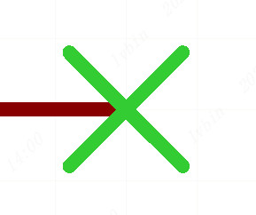 | 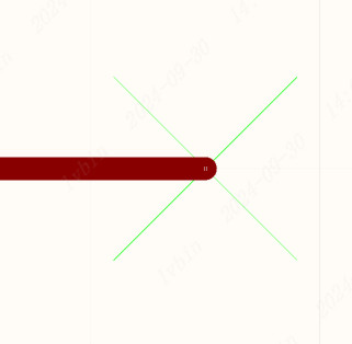 | - |
| Probe | Device | 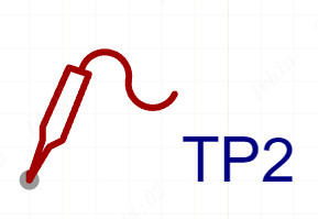 | 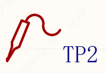 | - |
| Polyline | Drawing Tool - Line |  | 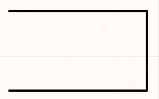 | - |
| Arc | Drawing Tool - Arc | 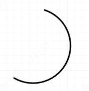 | 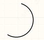 | - |
| Bezier Curve | Drawing Tool - Bezier Curve | 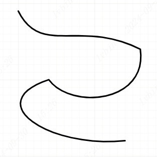 | 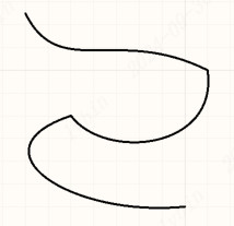 | - |
| Circle | Drawing Tool - Circle | 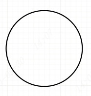 | 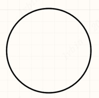 | - |
| Ellipse | Drawing Tool - Ellipse | 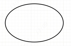 | 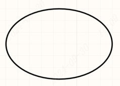 | - |
| Rectangle | Drawing Tool - Rectangle | 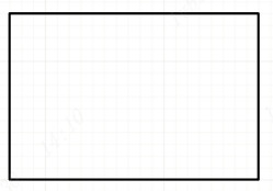 | 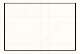 | - |
| Text | Text String |  |  | - |
| Table | Drawing Tool - Line | 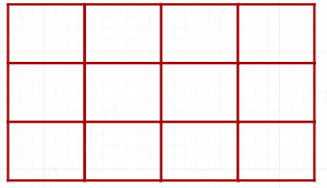 | 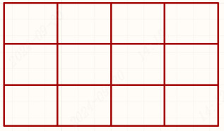 | Composed of multiple polyline segments to form a grid after conversion |
1.2. Unsupported Geometric Element/Function Types:
| Professional Layout Geometric Element/Function | Geometric Element/Function Description | Explanation |
|---|---|---|
| Short Circuit Identifier | Utilized for short-circuiting two distinct networks | Such an element does not exist in AD. |
| Image | - | The images in AD are saved locally and export is not supported for the time being. |
| Combination | Corresponding to the union in AD | Export of union information will be supported in subsequent versions. However, as the AD union name is not stored in the engineering data, export of the combination name is not feasible. |
| Component Masking | Masking types include "Add to BOM" and "Go to PCB" | Export is not supported for the moment. |
1.3. Geometric Element Differences
1.3.1. Line Width Conversion Discrepancies
- Included Objects: Wires, buses, polylines, arcs, Bézier curves, circles, ellipses, rectangles, and tables.
- Difference Explanation: The line widths of AD schematic geometric elements are mostly supported by Smallest**, Small, Medium, and Large. Line widths that are not supported will be converted to the closest width upon export.
1.3.2. Linear Type Conversion Discrepancies
- Included Objects: Wires, buses, polylines, arcs, Bézier curves, circles, ellipses, and rectangles.
- Difference Explanation: For the time being, only solid lines are supported for export. Other linear types will be converted to solid lines after export.
1.3.3. Font Conversion Discrepancies
- Included Objects: Attributes, attribute values, names, network labels, and text.
- Difference Explanation:
- a. The font after export may vary. Simultaneously, due to font differences, there may be minor displacements of the geometric elements.
b. If the same font is used in the export, due to the dissimilar logic of font display, it may not be completely consistent with the original file. There may be position shifts and size differences.
c. Export of text styles (bold, italic, underline) is not supported for the time being.
1.3.4. Discrepancies in Connection Point Style Transformations
Included Objects: Components (component pins), wires, network identifiers, network labels, network ports, probes.
Discrepancy Explanation:
a. Due to the inherent differences of the geometric elements, the styles of some component connection points may vary after transformation.
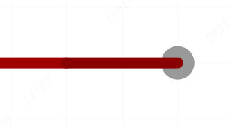
Professional Version Pin Connection Point Style 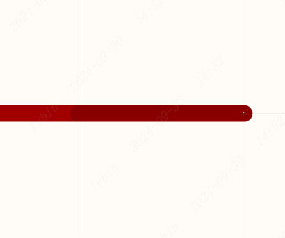
Exported Pin Connection Point Style 
Professional Version Network Label Connection Point Style 
Exported Network Label Connection Point Style 1.3.5. Filling Transformation Discrepancies
Included Objects: Polyline, arc, Bézier curve, circle, table.
Discrepancy Explanation: The above geometric elements do not support the export of filling for the time being.
1.3.6. Component Conversion Discrepancies
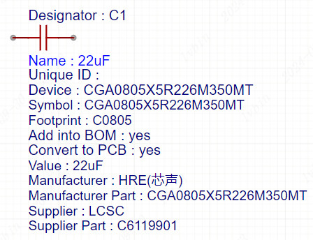
- Components are composed of multiple symbol elements as composite elements, and any difference in symbol elements may cause conversion differences for the components.
- AD does not support the display of basic attribute names, and only attribute values are shown after conversion.
- Some attribute values are not displayed after conversion.
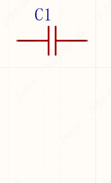
1.3.7. Discrepancies in Network Tag Conversion
- There are differences in the graphic element styles after conversion.
- The graphic element style of the protective ground will be converted to the analog ground after export, and it will be rectified subsequently.
- In some cases, VCC will be lost after conversion, and it will also be rectified later.


2. PCB2.1. Supported Graphic Element Types
| AD Graphic Element | After Import | AD Graphic Element Style | Converted Graphic Element Style | Explanation |
|---|---|---|---|---|
| Component | Device | 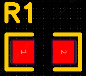 | 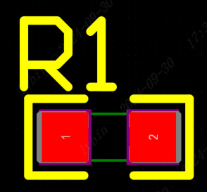 | - |
| Via | Via | 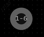 | 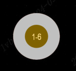 | The graphic element style differs. |
| Non-standard Pad | Region, Pad | 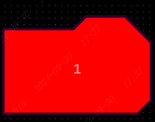 | 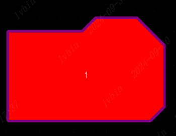 | - |
| Board Outline | Keepout | 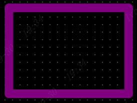 | 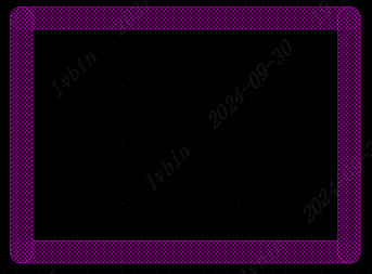 | AD has no board outline graphic element. After export, it is converted to Keepout of the Board Outline Layer, with restrictions including via holes, track lines, copper fills, SMD pads, and TH pads. |
| Fill Area | Region | 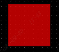 | 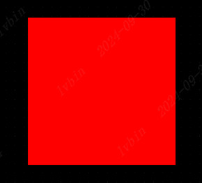 | - |
| Copper Pour Area | Copper Pour | 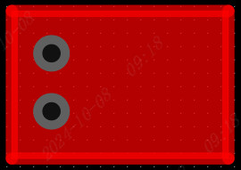 | 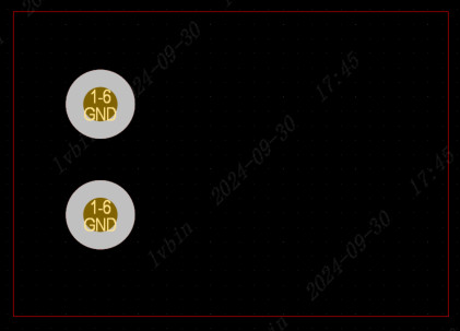 | PCB copper pour filling is not supported for export and needs to be manually recreated in Altium Designer after export. |
| Slot Area | Keepout - Region | 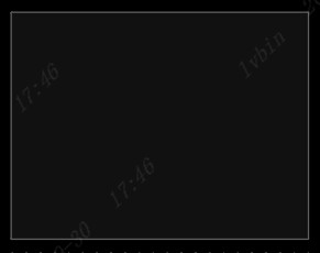 | 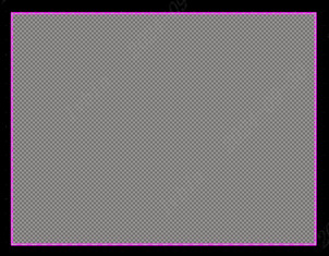 | Converted to multi-layer Keepout - Region, with no restricted objects. |
| Constraint Area | Keepout - Region | 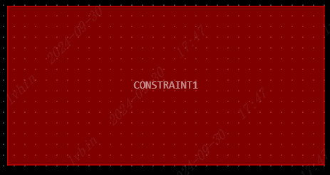 | 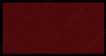 | Converted to the corresponding layer's Keepout - Region, with no restricted objects. |
| Prohibited Area | Keepout - Region | 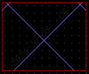 |  | Due to the difference between the prohibited options of the prohibited area and the restricted objects of Keepout, it is temporarily not exported. |
| Polyline | Track | 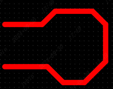 | 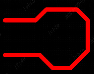 | - |
| Arc | Arc | 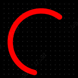 | 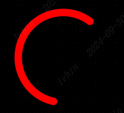 | - |
| Test Point | Pad | 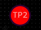 |  | - |
| Reinforcement | Region | 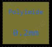 | 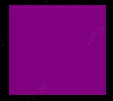 | Converted to Region of mechanical layer 2, with the type being Copper. |
| Text | String |  |  | - |
| Image | Device | 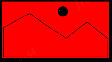 | 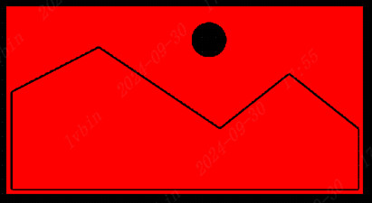 | Non-original images are exported as devices. Since AD does not support color silkscreen printing, the original images are not supported for export. |
| Length Dimension | Dimension |  | 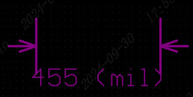 | The graphic element style of the dimension differs after export. |
| Stackup/Drill Table | Wire and String | - | - | Composed of wires and strings to form a composite graphic element for export. The table border is made of wires, and the text content is a string. |
| Inner Electrical Layer | Inner Electrical Layer | - | - | The inner electrical layer area of the PCB cannot be completely consistent when exported and requires manual adjustment and reconstruction. |
Note: Some layers of the PCB cannot be accurately mapped to the corresponding layers in Altium and will be exported in more mechanical layers.
2.2. Unsupported Graphic Element Types:
| Professional Graphic Element/Function | Graphic Element/Function Description | Explanation |
|---|---|---|
| 3D Enclosure | Comprising frame, screw columns, side reference lines, side milling areas, top/bottom milling areas, side solids, and top/bottom solids. | This graphic element is not supported in AD and cannot be exported. |
| Color Silk Screen Printing | Including silk screen printing colors and color pictures | Color silk screen printing is not supported in AD. The silk screen printing colors are lost after export, and color pictures are not supported for export. |
| Angle Dimensions/Radius Dimensions | - | The styles of graphic elements differ significantly and are not supported for export at present. |
| Copper Pour Fill | The copper pour fill area within the copper pour region | The copper pour fill of PCB is not supported for export. After export, all copper pours need to be manually recreated in Altium Designer. |
| Combination | Corresponding to the combination in AD | Export of combination information will be supported in subsequent versions. However, as the combination name in AD is not stored in the engineering data, the export of combination names is not supported. |
| Buried Vias | - | It becomes copper pour vias after export. |
2.3. Shape Discrepancies
2.3.1. Discrepancies in Font Conversion
- Included objects: attributes, attribute values, names, dimensions, and text
- Explanation of differences: - a. The font may differ after export. Simultaneously, due to the variance in fonts, slight displacements of the graphic elements might occur. - b. If the same font is used upon export, due to the dissimilar logic of font display, it cannot be completely consistent with the original file, and there may be positional offsets and size differences.
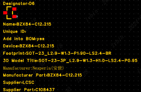
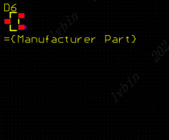
2.3.2. Discrepancies in Component Conversion
- Components are composed of multiple packaged graphic elements. Any difference in the packaged graphic elements may lead to conversion discrepancies of the components.
- AD does not support the display of basic attribute names.
- Attribute values, except for the position number, may be lost or displayed abnormally after export.
2.3.3. Discrepancies in Converting Irregular Pads
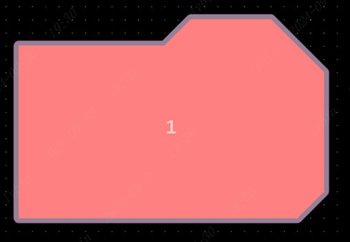
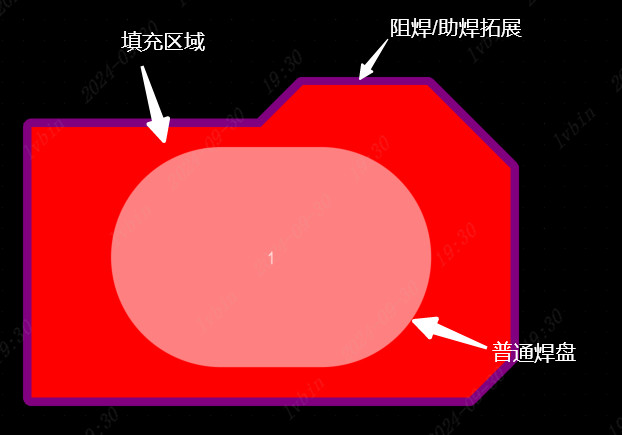
- AD does not support irregular pads. Irregular pads are exported as a composite primitive composed of a common pad and a filling area. The solder mask and solder assist expansion in the irregular pad are achieved by the filling area.
2.4. Design Rules
2.4.1. Design Rule Export Comparison Table:
| Design Rules in the Professional Edition | Corresponding Design Rules after Import | Explanation | |
|---|---|---|---|
| Spacing | Clearance | Electrical-Clearance | - |
| Other Spacing | - | Import of Hole To Hole Clearance will be supported in the future. | |
| Physical | Conductor | Routing-Width | - |
| Network Length | - | - | |
| Differential Pair | Routing-Differential Pairs Routing | In the Professional Edition, setting different differential pair rules for different layers is not supported. After export, the differential pair design rules for all routing layers are consistent. The maximum gap after export is the default gap. | |
| Blind/Buried Via | - | - | |
| Via Size | Routing-Routing Via Style | - | |
| Plane | Internal Power Layer | Plane-Power Plane Connect Style | AD does not support setting the divergence angle. After export, the divergence angle is 45°. |
| Routing-RoutingLayers | After export, the internal power layer becomes a layer not allowed for routing. | ||
| Copper Pour | Plane-Polygon Connect Style | For the time being, only simple constraint design rules are exported. Export of advanced constraint design rules will be supported in the future. | |
| Expansion | Solder Mask Expansion | Mask-Solder Mask Expansion | The external expansion constraint data adopts the pad external expansion constraint data. |
| Paste Mask Expansion | Mask-Paste Mask Expansion | The external expansion constraint data adopts the top layer external expansion constraint data of the pad, and the usage range is for SMD pads with the paste mask layer. | |
| Fanout | - | - | The rules have significant differences and export is not supported for the moment. |
2.4.2. Safety Clearance Export Comparison Table:
| Elements in the Professional Edition | Corresponding AD Elements after Export | Explanation |
|---|---|---|
| - | Arc | After export, the safety clearance of Arc to all elements is taken as the safety clearance between lines. |
| Trace | Track | - |
| SMD Pad | SMD Pad | - |
| TH Pad | TH Pad | - |
| Via | Via | - |
| Fill Area / Teardrop | Fill | - |
| Slot Area | Region | - |
| Line | Poly | - |
| Text / Picture | Text | - |
| Board Outline | - | Support will be provided in subsequent versions. |
| Drilling Hole | Hole | - |