PCB FAQ
How to modify the unit on PCB
Details
You can use the shortcut key Q

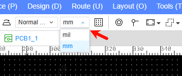
You can click the unit switch drop-down on the top toolbar
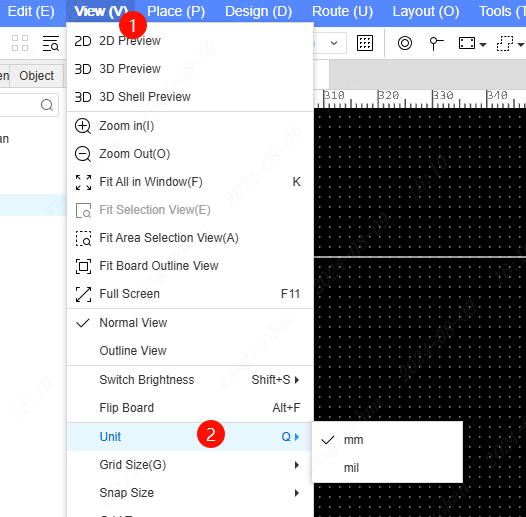
You can click the top menu - View - Unit to switch
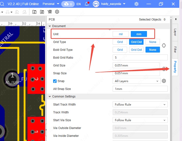
You can also modify it in the property bar on the right side of the PCB interface.
How to delete unwanted paste mask layers
Details
How to delete unwanted paste mask layers (steel mesh layer, soldering paste layer) in EasyEDA, here are two methods:
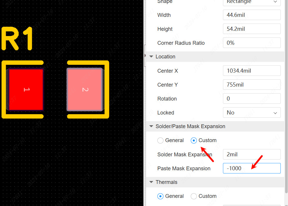
- Click the pad on the PCB, set the paste mask extension to custom for the pad, and set the value to -1000. When the paste mask extension is 0, the solder paste shape is the same size as the pad shape. When it is a negative number, it will be smaller than the pad shape.
If you don't want to set the pads one by one, you can set it directly in the design rules. The paste mask extension attribute of the pad is the general type (follow the rules) by default. 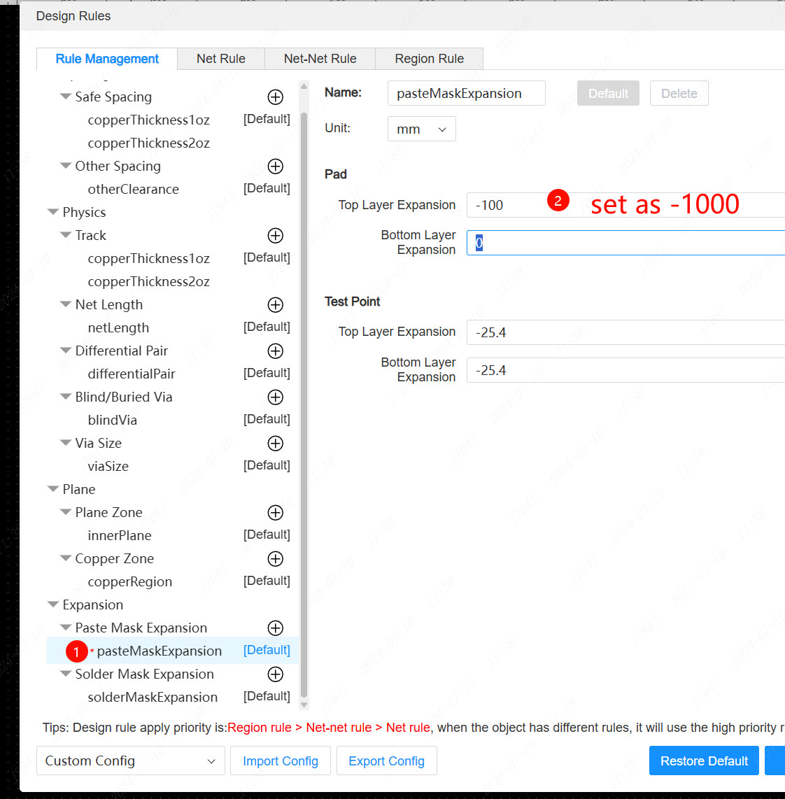
- When exporting Gerber, select custom export and uncheck the paste mask layer. Note: this will not export the entire paste mask layer! ! !
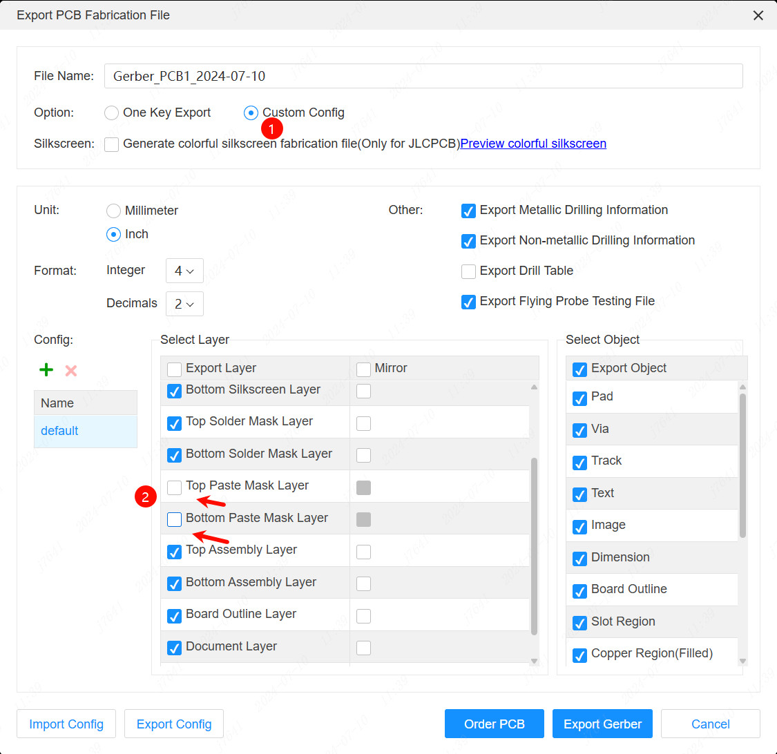
Similarly, if you do not need to cover the pad with green oil, you can make similar settings for the solder mask extension or solder mask layer.
How to convert copper region to fill region
Details
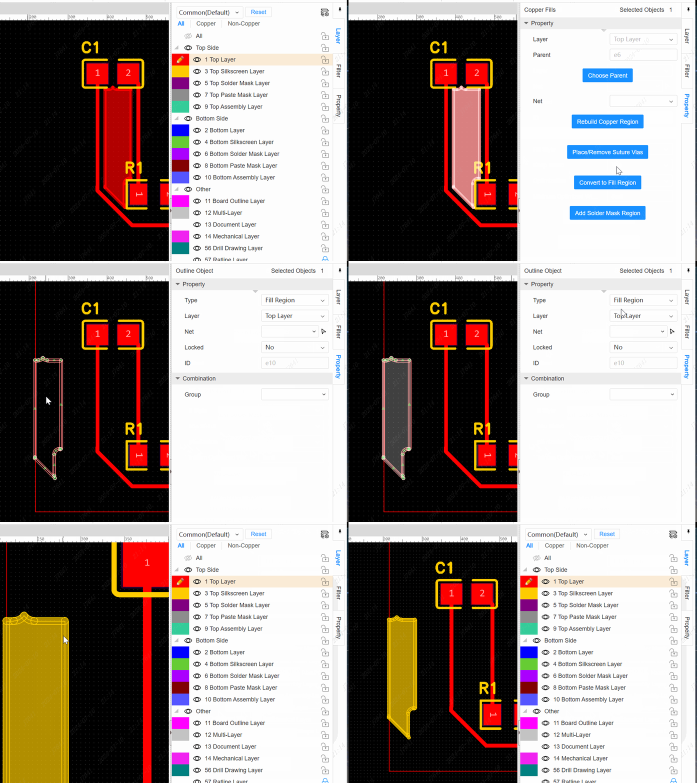
If you want to convert the dynamic copper shape to fill area so that it can be placed on the silk screen layer, etc., you can directly convert it to fill area in the copper fill property panel, and then switch the layer of the fill area.
The operation is as follows:
Draw copper within the border and keep the copper island
Click copper fill, you need to click the left button twice
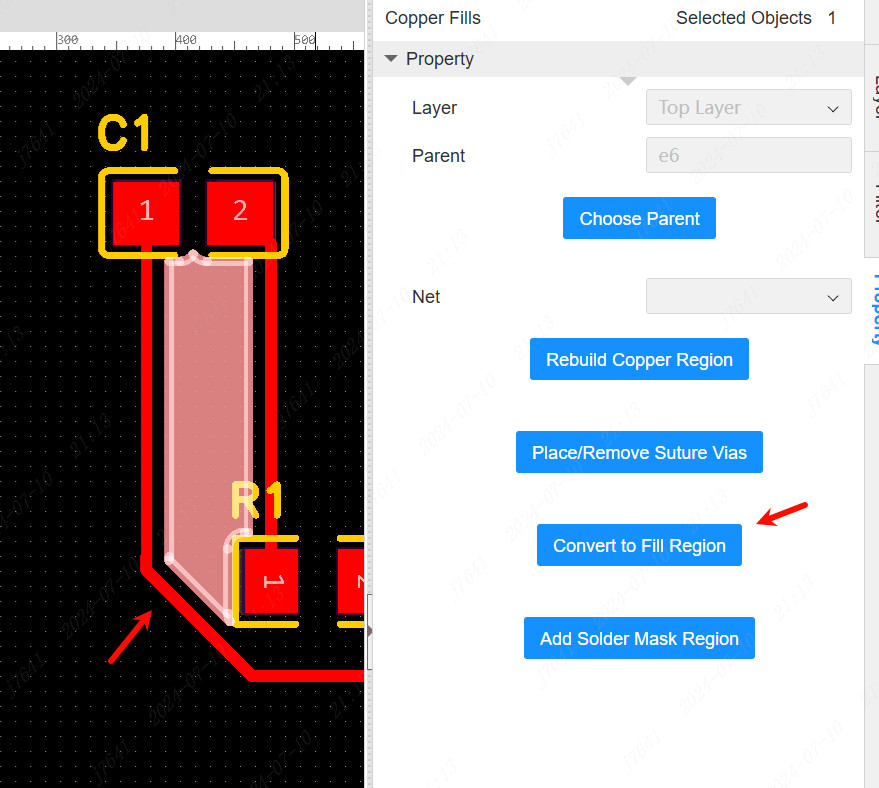
Click "Convert to fill area" in the right property panel
Cannot open PCB properly
Details
1, please ensure that the computer has a graphics card, and not very old graphics card. Because opening the PCB needs the support of the graphics card. 2, re-open the editor to try or log out (choose to remove the cache), if you still can not open, there may be data abnormalities, please contact technical support. 3, if the client, please use Google Chrome and start hardware acceleration. Currently found that some Win7 computer installation client can not properly open PCB, the browser is normal.
How to set design rules
Details
In the top menu - Design - Design Rules 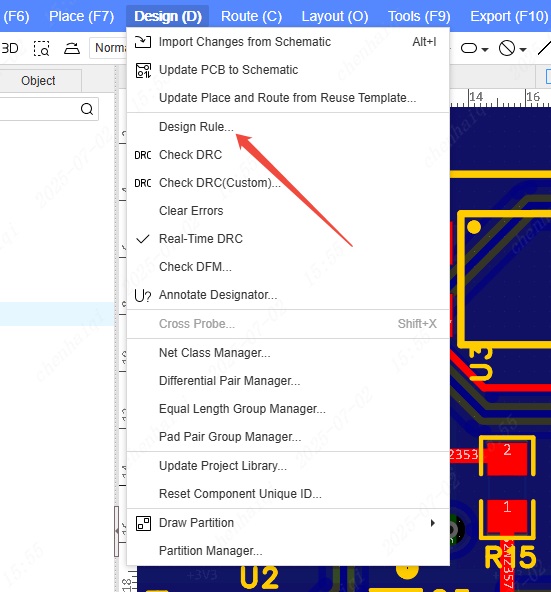
How to generate PCB order file
Details
In the Top Menu - Export - PCB Fabrication File Gerber 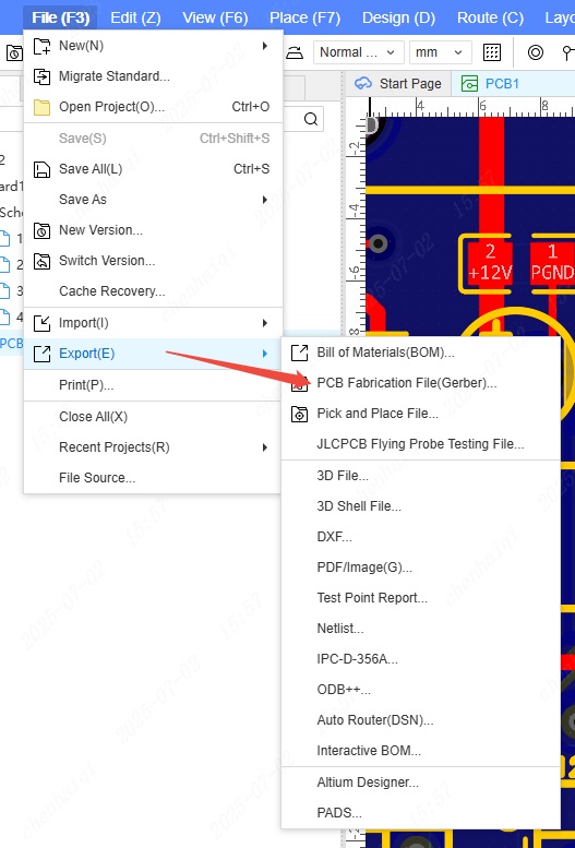
How to show/hidden copper
Details
You can hide all copper areas in the filter panel on the right, or hide a single copper area in the object column on the left. 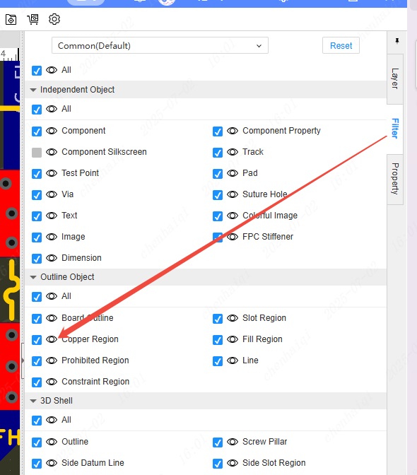
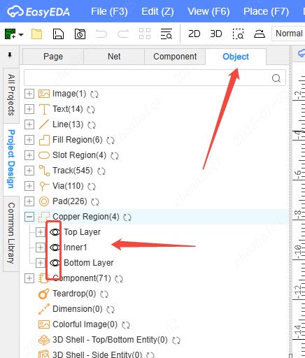
Add commonly used fonts
Details
Support setting your own commonly used fonts. These fonts need to be installed on the local computer to be called by the editor, otherwise the editor will automatically use the default font provided by the browser for rendering.
To add custom fonts. (1) Install the fonts you need on your local computer first, if you already have fonts, you can ignore this step.
(2) Take Windows system as an example, find the font settings inside the system settings and get the font name. You need to get the exact display name, not the file name of the font file. 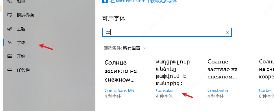
(3) Add a font according to the font name. 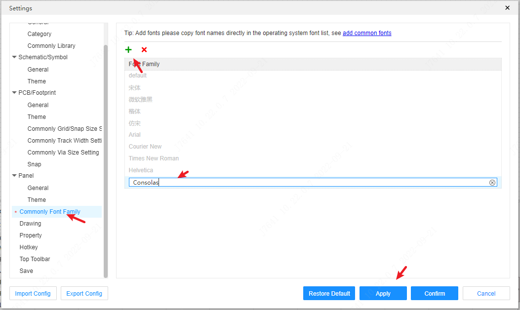
(4) You can see this font in the text font switch of the schematic or PCB, and you can switch the font at this time.
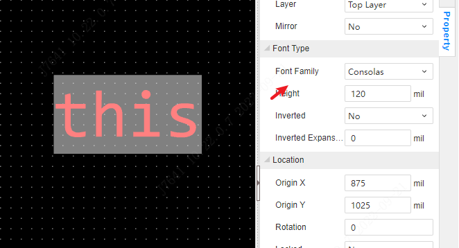
The added fonts can be used by schematics, panels, PCBs, etc.
How to add FPC?
Details
Three shapes can be found and placed in the top menu bar. Top Menu Bar - Place - FPC Stiffener It should be noted that only the professional version has the function of adding FPC, the standard version does not. 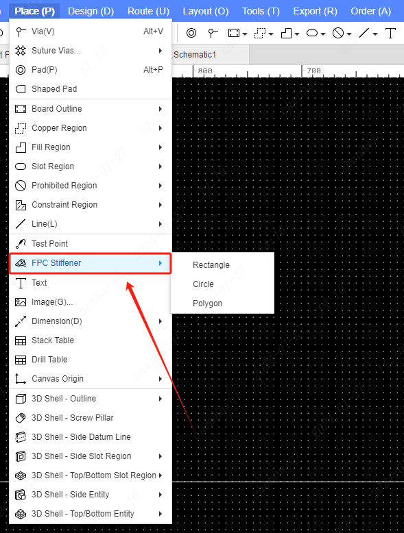
How to clone?
Details
Only borad, schematic diagram, PCB can be right-click to select clone. 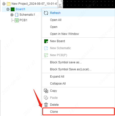
How to place the Slot Region?
Details
Place in the top menu bar.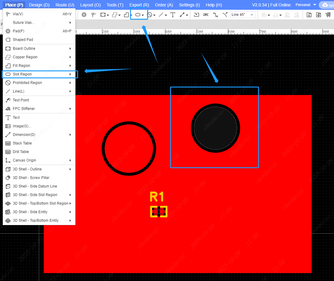 Please refer:https://prodocs.easyeda.com/en/pcb/place-slot-region/
How to place Prohibited Region?
Details
Start by finding the Prohibited Region in the top menu bar and select the element you want to disable.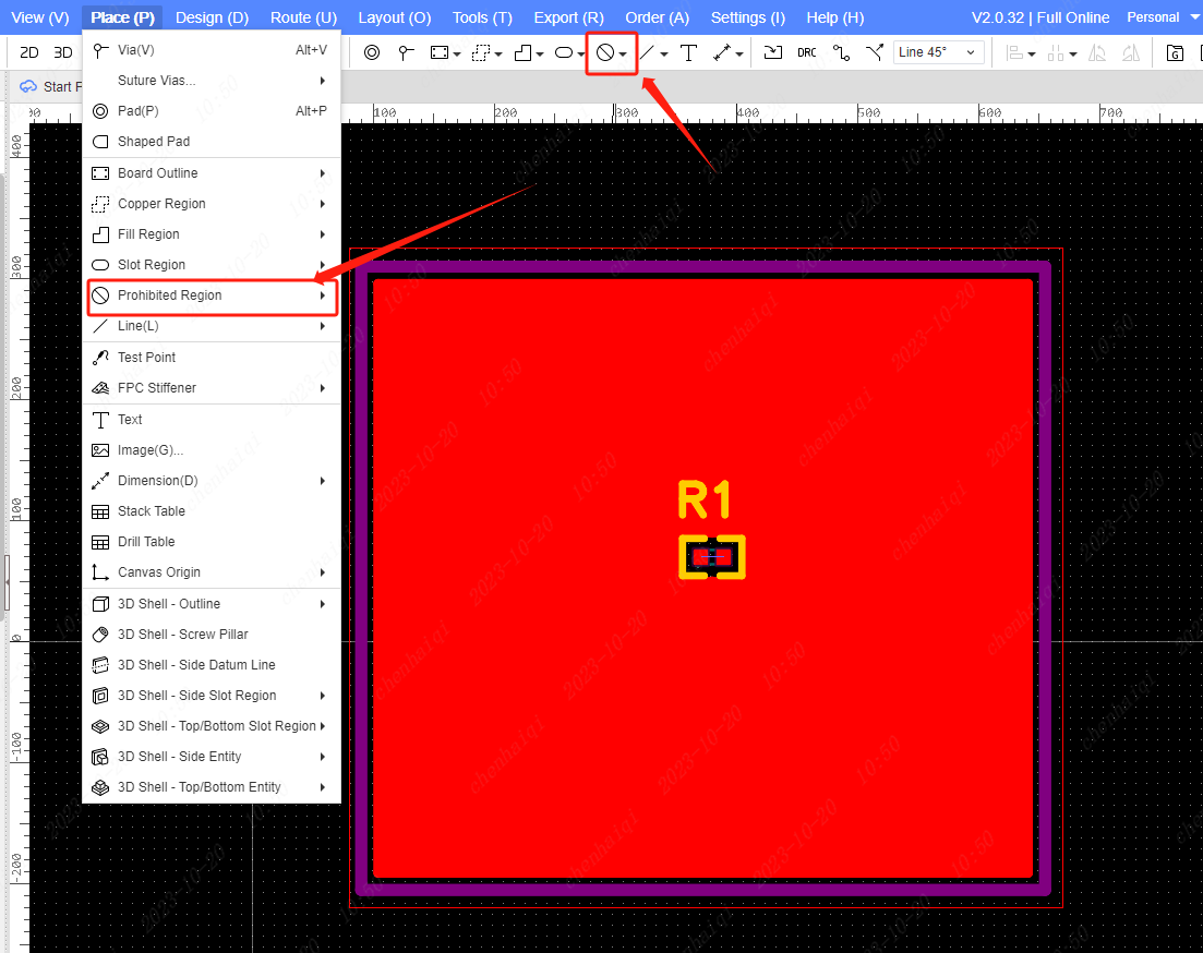 Please refer:https://prodocs.easyeda.com/en/pcb/place-prohibited-region/
How to batch change font size in pcb?
Details
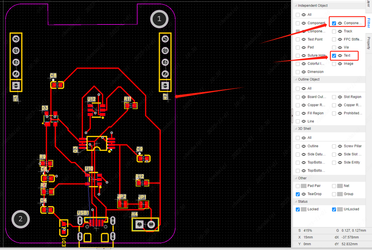
The first option: Change the default Settings. After this change is made, all fonts used will be set according to this standard. 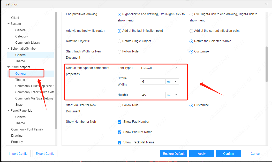 The second option, select all the text and modify it in the properties bar on the right. This method works for all components that have been placed, but the modified Settings only exist in the current pcb.
How to modify the “plated”of the pad?
Details
Select the pads to select them in the Properties column on the right. It should be noted that once the ‘plated’ setting of the pad is set to ‘no’, the pad loses its electrical properties and the inner wall of the through-hole is copper-free.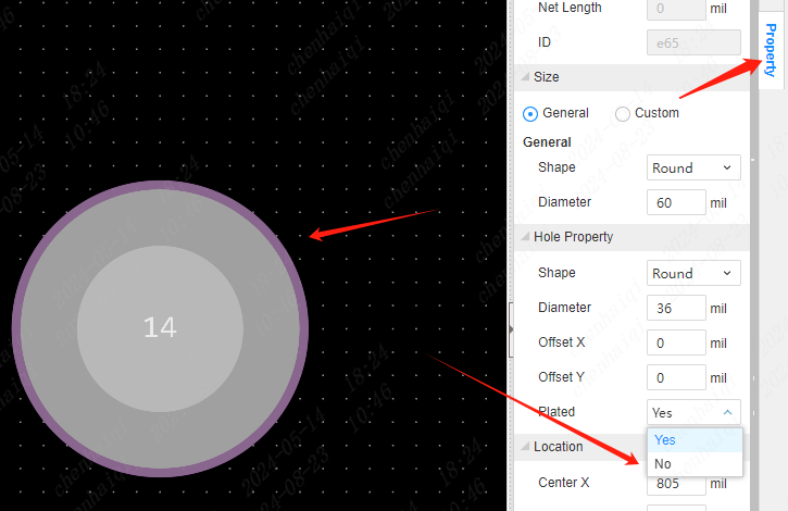
How to change the zoom of the editor?
Details
Generally the system default zoom is to scroll the mouse wheel to control the zoom size. You can change the zoom method in the “Setting” on the top menu bar. 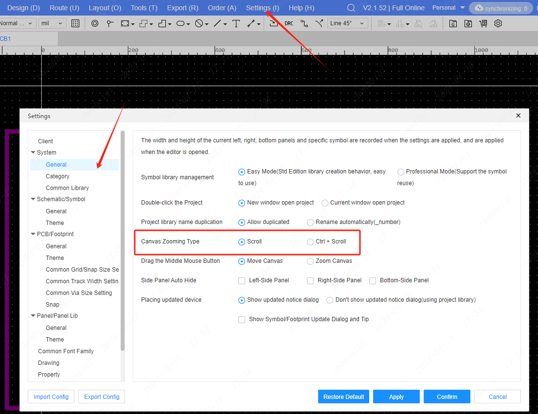
How to modify the line width during the wiring process?
Details
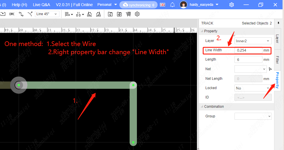
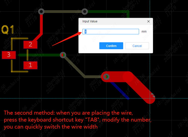
How to solve the problem of Ratlines after copper is paved?
Details
First of all, this is because the copper skin has a gap, so you need to place a wire or a hole to connect. In the first method, after the top layer of copper is finished, it is necessary to continue the bottom layer of copper. After the copper laying is completed, two vias are placed near the two end components.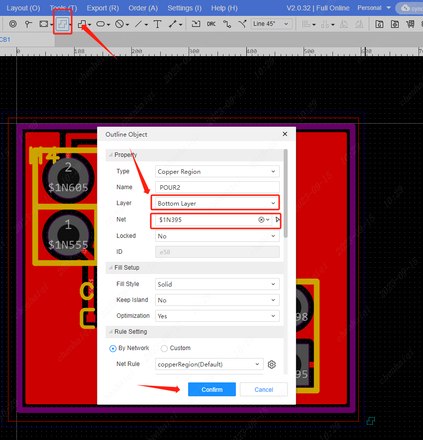
The top and bottom layers of the copper network must be consistent.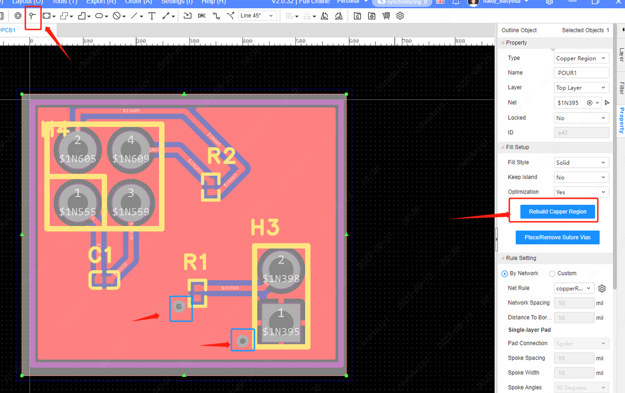
After placing the vias, both the top and bottom layers must "Rebuild the Copper Region". The second way is to use wires and vias to rewire and connect the bottom layer to the top layer. It is necessary to finish the top and bottom layer of copper before connecting.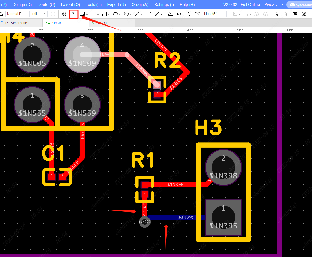
How to add a solder mask to the vias or pads?
Details
First select the vias or pads. Find "property" in the right menu bar, and set the value of the top and bottom solder mask extensions respectively. The larger the value, the larger the copper leakage of the window.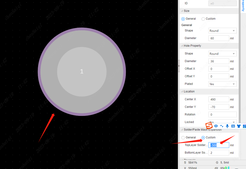
How to modify the rules for connecting copper area to pads?
Details
Firstly, select the ‘Design’ window in the top menu bar to access the ‘Design Rule’ function.Then select ‘Copper Zone’ to enter the design rule interface to modify the copper laying rules.And you can modify the connection types.There are three connection types to choose from: Spoke, Direct, and No Connection.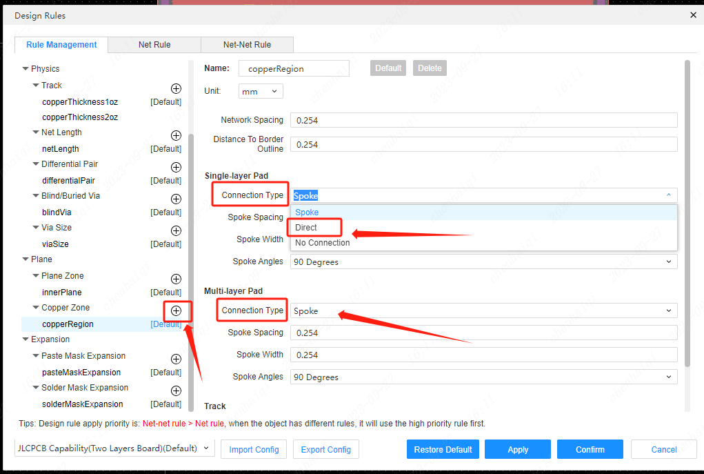
How to use Boolean Operation to draw the fill area of the circle?
Details
First draw two circular fill regions.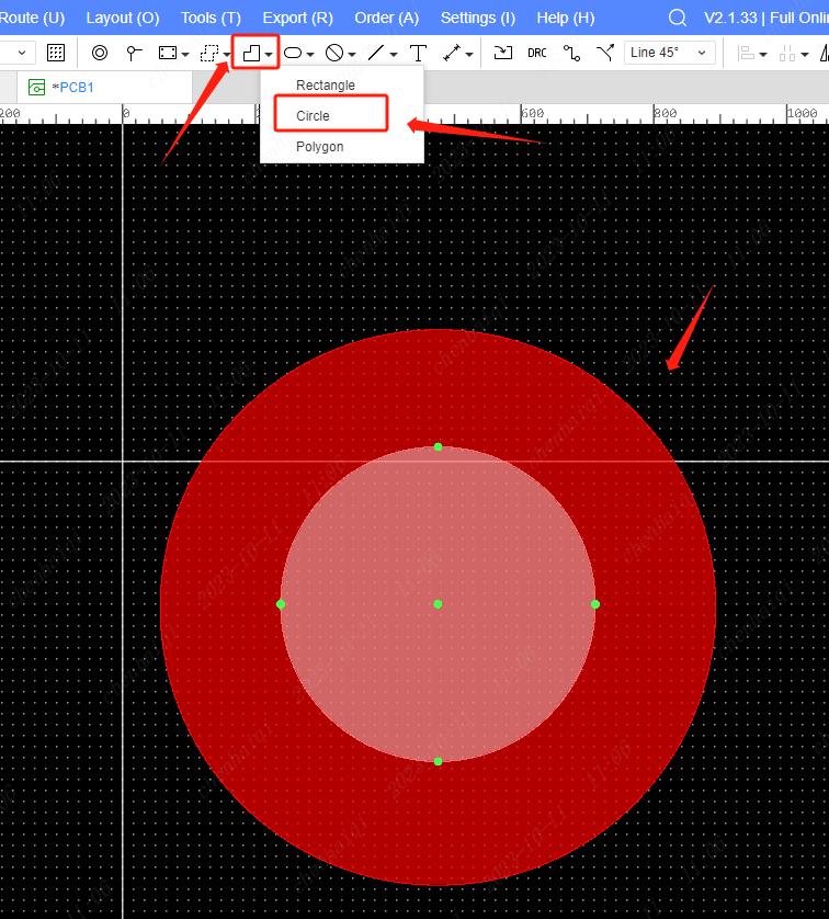
Then selected elements in the frame and use Boolean Operation's "Exclude Overlapping Areas" function. Note: Only Fill Regions can use Boolean Operation.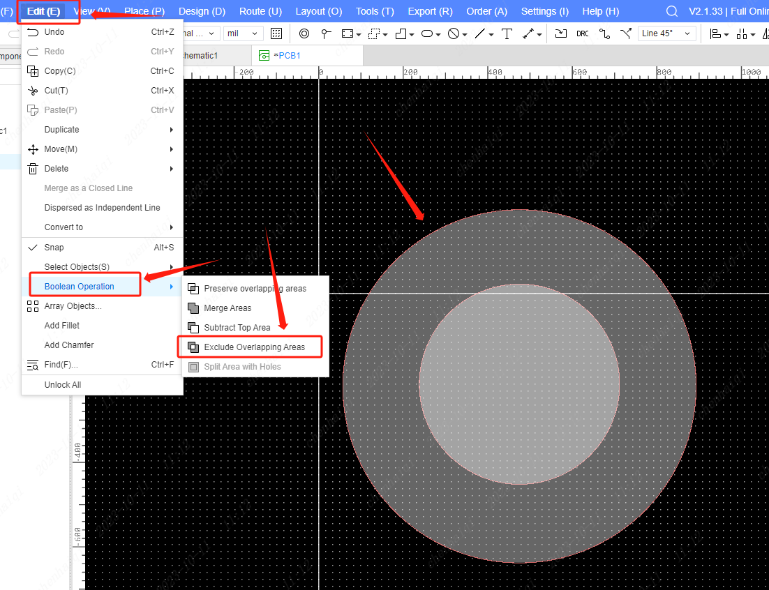
You can also use other functions to achieve the effect of overlap.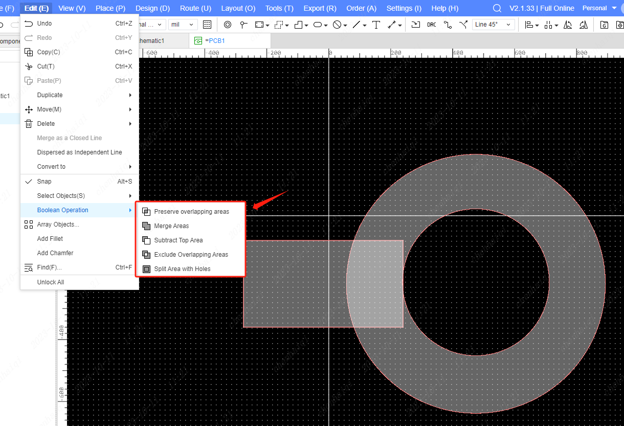
Why not show it after laying copper?
Details
There are the following reasons for not being displayed after the copper paving:
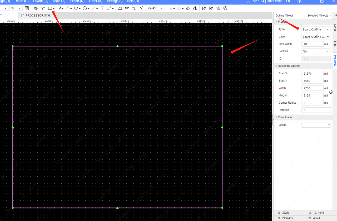
Check whether the Board Outline Layer is completely closed.
Whether the copper network has the same network on the PCB board.
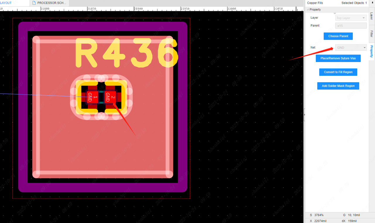
If there is no network inside copper or the network is different, then you can click on the copper line frame, and then modify the attribute "Keep Island" in the attribute bar on the right attribute bar to "Yes".
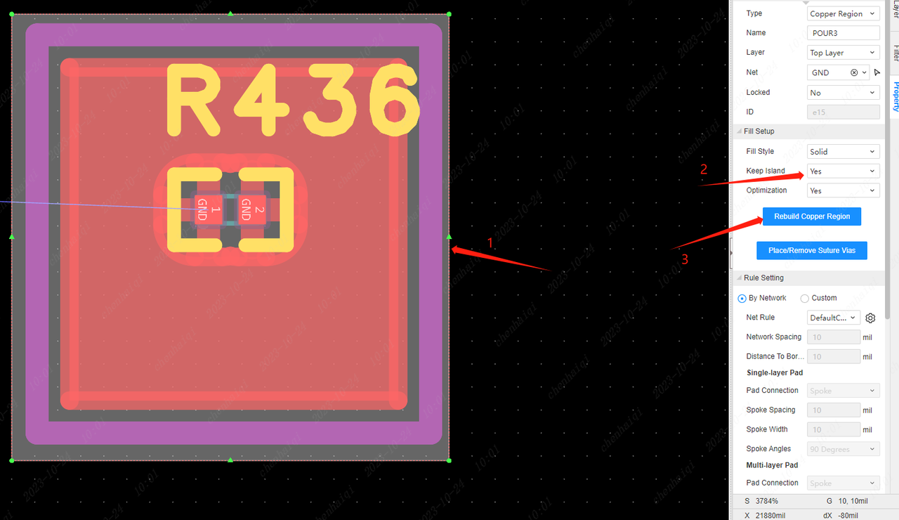
If the small piece of copper is not displayed, then move the small copper that is not displayed in the Copper Manager can be moved to the large copper. Please refer:https://prodocs.easyeda.com/en/pcb/tools-copper-manager/
Check if the "eye" is opened inside the filter.
How to select all wires in bulk and change wire width?
Details
Check the wires individually inside the filter.Then select the entire pcb and it will automatically filter out all wires. The last thing you need to do is change the attribute.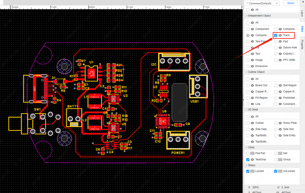
How to add fillet?
Details
Select the desired line segment, click the right mouse button, select ‘Add’ inside the ‘add fillet’ function can be completed to add. 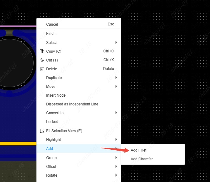
How to draw v-cuts?
Details
Use the polyline of the Board Outine Layer to draw an extension line where the V cut is needed. You may choose to use text alongside the words "v-cut" or not.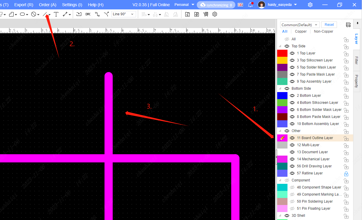
How to remove green oil from copper area?
Details
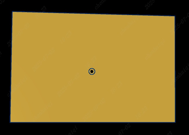
Select the internal area of the copper plating, and then click the "Add Solder Mask Region" tool in the property bar on the right. 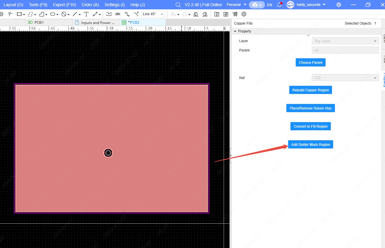
How to remove the inner layer?
Details
You can try the following ways to deal with the error reported when deleting the internal electrical layer: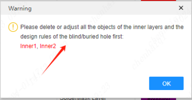 Step 1: Hide all layers and show only the inner layers.
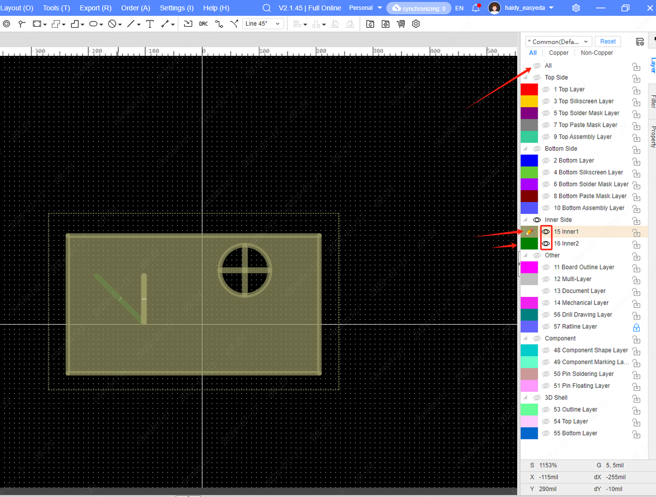 If you are blind via ,and you need to open the multilayer.
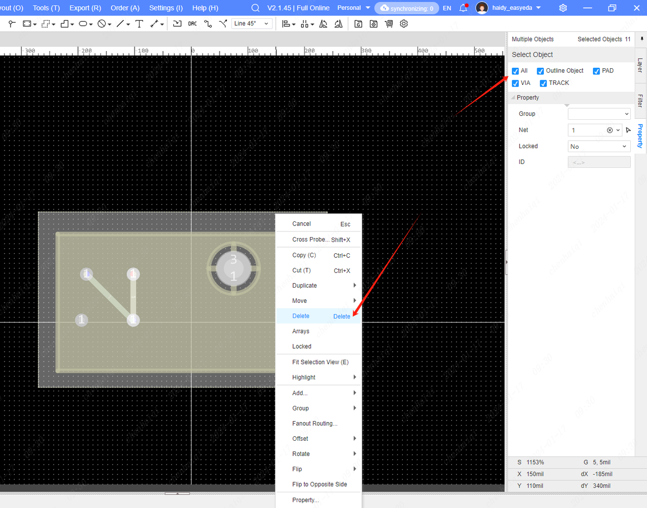
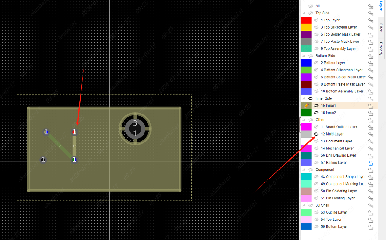 Select All to remove all elements.
Step 2: Delete all the blind hole design rules in the design rules.After both steps are done, you can go back to the Layer manager and change the multi-layer board to a 2-layer board.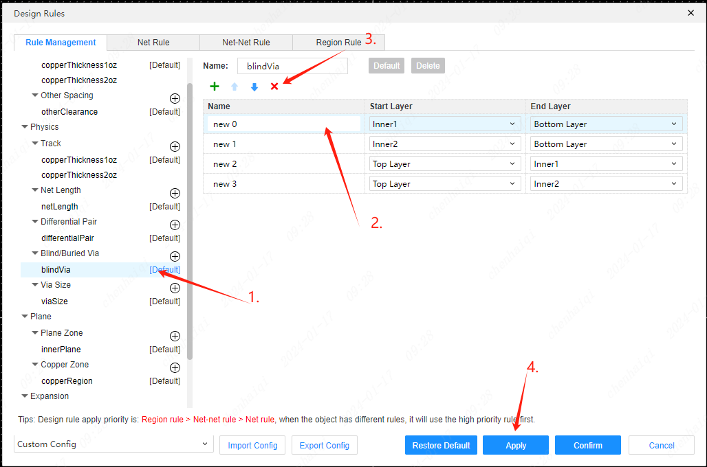
How to set the position of component Designator in bulk?
Details
The Property Location function can be found in the top menu bar.Also, in the schematic you can find and use the Property Location function.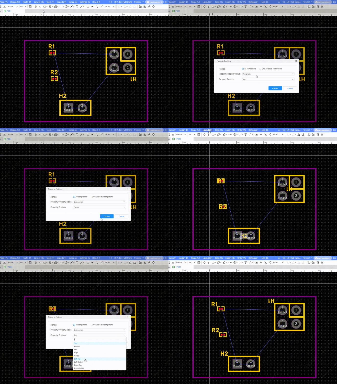
How to make square pads?
Details
Currently we are only able to support the creation of square multilayer pads, but not square drilled multilayer pads. When we need to make square multilayer pads, we can change the shape by selecting the pads and then changing the shape in the property bar on the right. 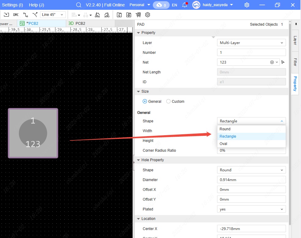
What should I do when the 3D preview doesn't show the board effect?
Details
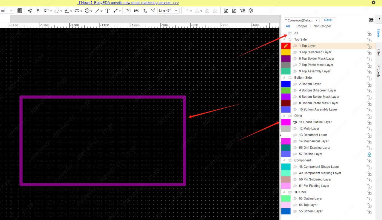
Check the Board Outline Layer if the board effect is not shown in the 3D preview after the PCB is drawn. You need to check that the endpoints between Board Outlines are closed and that there are no overlapping Board Outlines. If there are dispersed line segments, you need to close them all as a whole. If there are overlapping segments, they need to be deleted.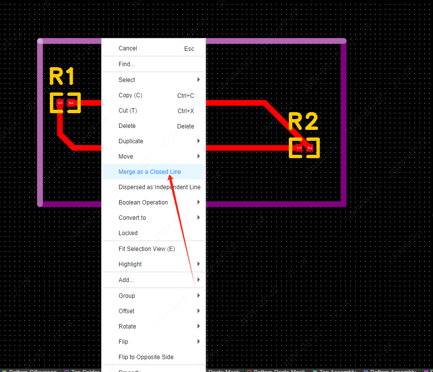 You can hide all the layers and then view them with only the Board Outline displayed to scrutinize each line segment.
How does the wire leak copper?
Details
Select a wire, click the right mouse button and select Add Soldermask.You can then see in the 3d preview that the wire showing yellow is the effect of leaking copper skin. 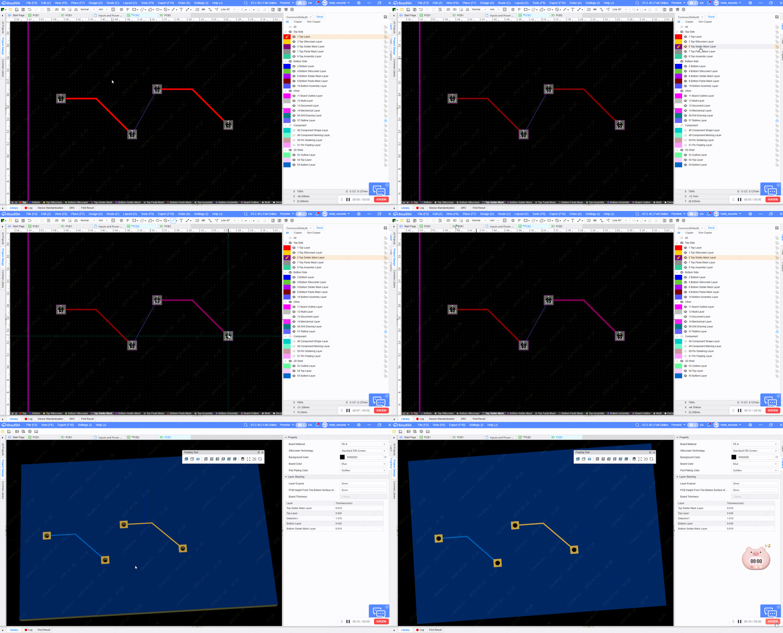
How to remove the green oil from the surface of the board?
Details
How can I get rid of the green oil on the surface of the board when no copper-laying area is used in the PCB? Select Draw a piece of Fill region Set its layer as top soldermask layer and then preview it in 3d to see the effect.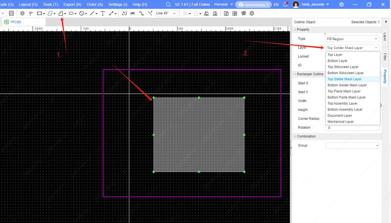
How to change the colour of the ratline?
Details
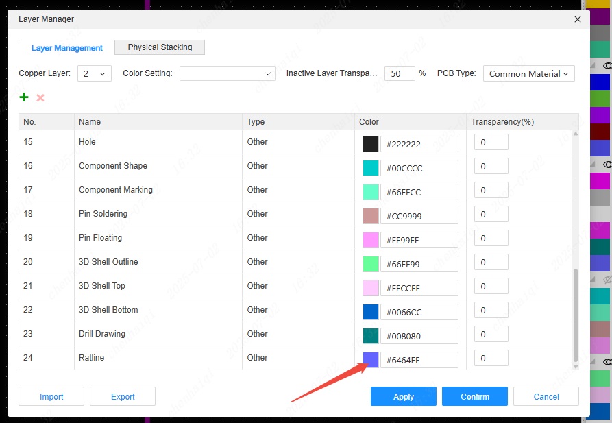
Go to the Layer Manager from the top menu bar, then find the ratline layer and change the color of that layer. Note that you can only change the colors of all ratlines, not the colors of individual ratlines. 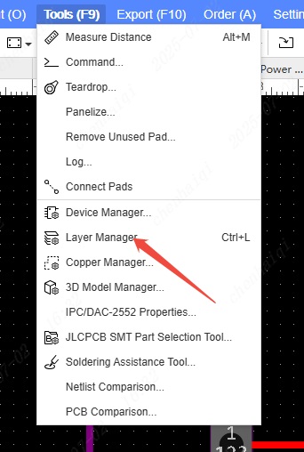
How to change the wire colour for a particular network?
Details
If you want to modify the wires of a network individually, you can find the "Net" toolbar in the left panel of the PCB interface.Then you can change the colour of the network name you want to modify.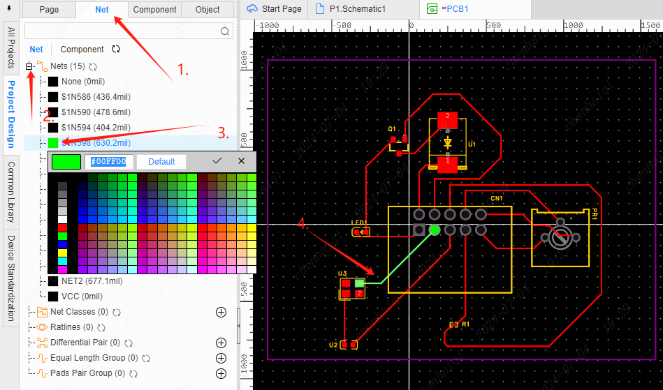
How to solve the DRC error reporting free copper region in the internal electric layer?
Details
 This is what you can do when ‘free copper region error’ occurs: Step 1: Place the brush on the inner electric layer.
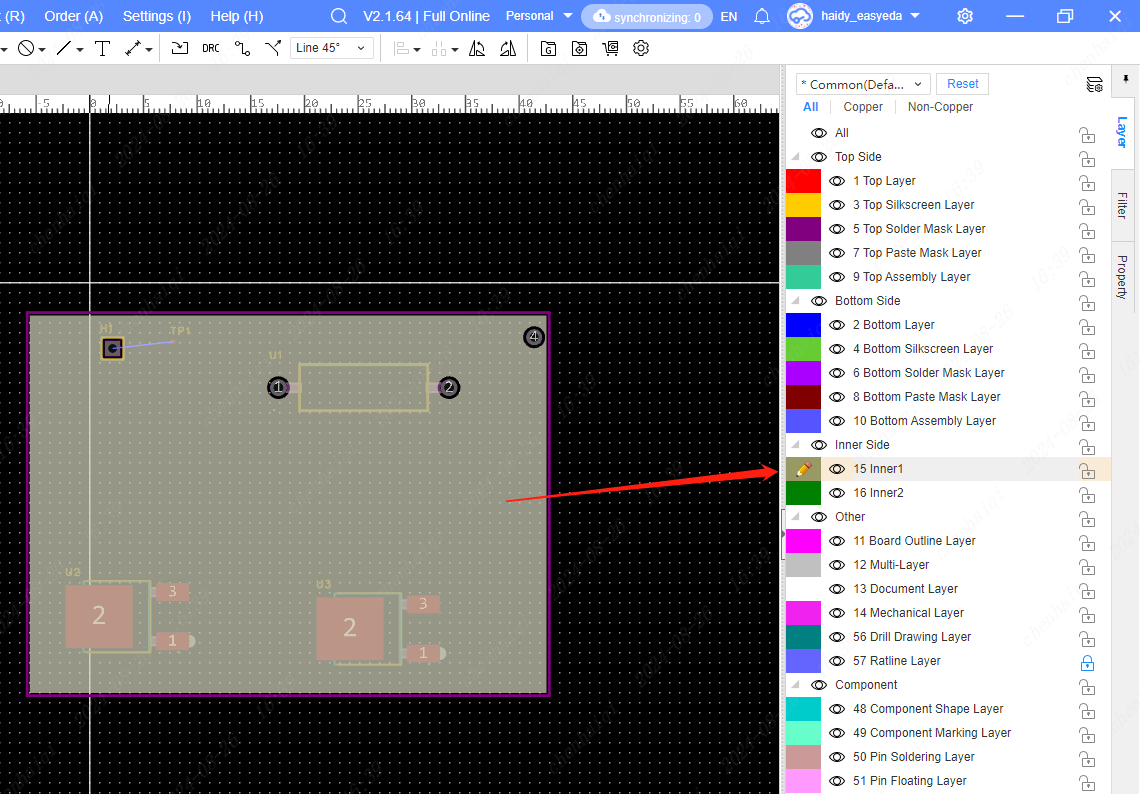
Step 2: Click to select the inner layer area and set ‘Keep Island’' to “No” in the right property bar.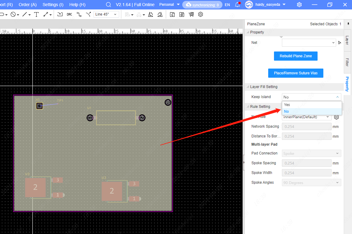
All problems with the error ‘free copper region’ can be solved in this way.
How is the inner layer partitioned?
Details
You need to use the folding tool in the inner layer, rebuild the inner electric layer after drawing, shift+b to achieve partitioning, and then click on Set Network.Note that you need to select Retain Silos to enable partitioning.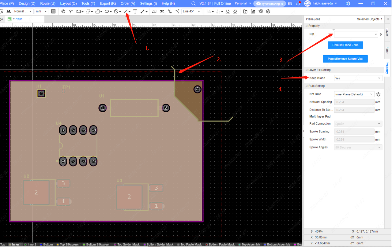
Minimum Track Corners
Details
- During the wiring process, if there are three adjacent segments of undefined wires (including undefined wires after automatic setback), and the first and third segments form a right angle, the middle segment of the wire needs to meet the value of the ‘Minimum Track Corners’ setting. The value can be set from 0 to 100, and is supported to 1 decimal place.
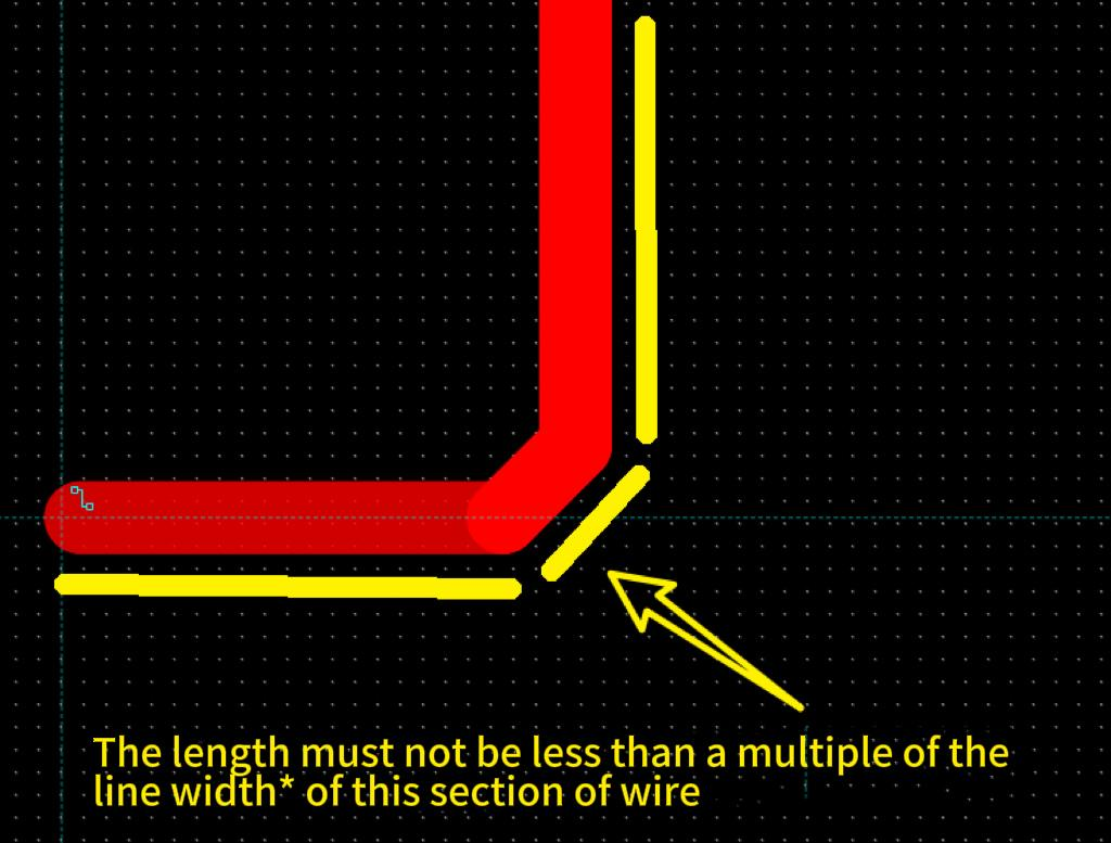 1.1 There may be more than one conductor in an undetermined segment that satisfies this relationship
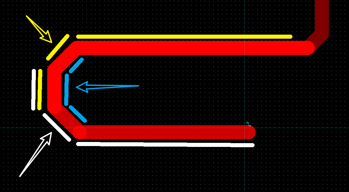
1.2 Starts adding inflection points when the set length is not reached 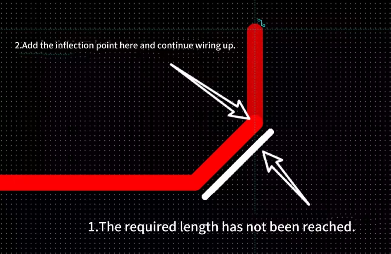
1.3 After adding an inflection point, back off this and the previous inflection point, and start planning a new wire from the previous inflection point. However, there are still wire segments in the re-generated wire that do not meet the minimum corner requirements, so it is necessary to continue to fall back the wire segments forward until the rules are met. 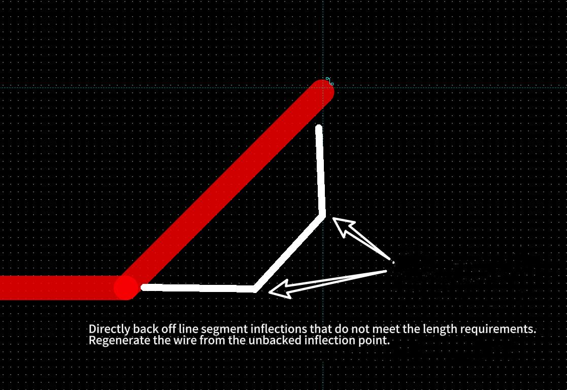
1.4 However, if you add an inflection point and then continue wiring to the right, you need to continue pulling segments from this inflection point, which means that the above logic only applies if you continue wiring upwards to form 90 degrees. 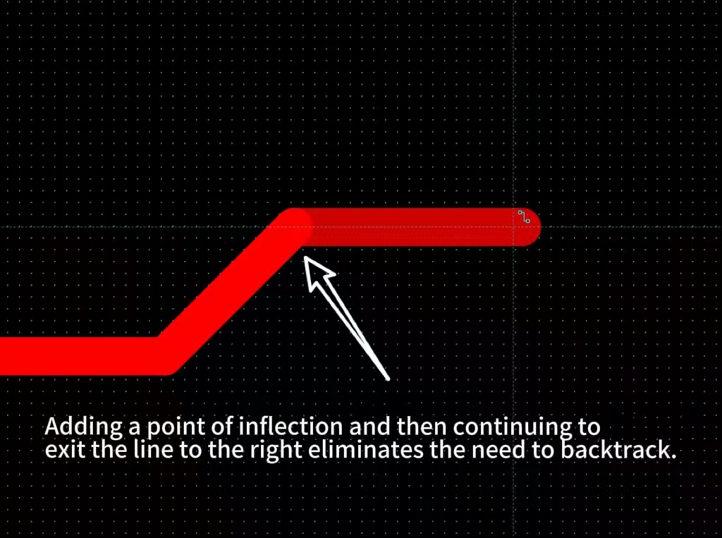
1.5 Special scenarios. 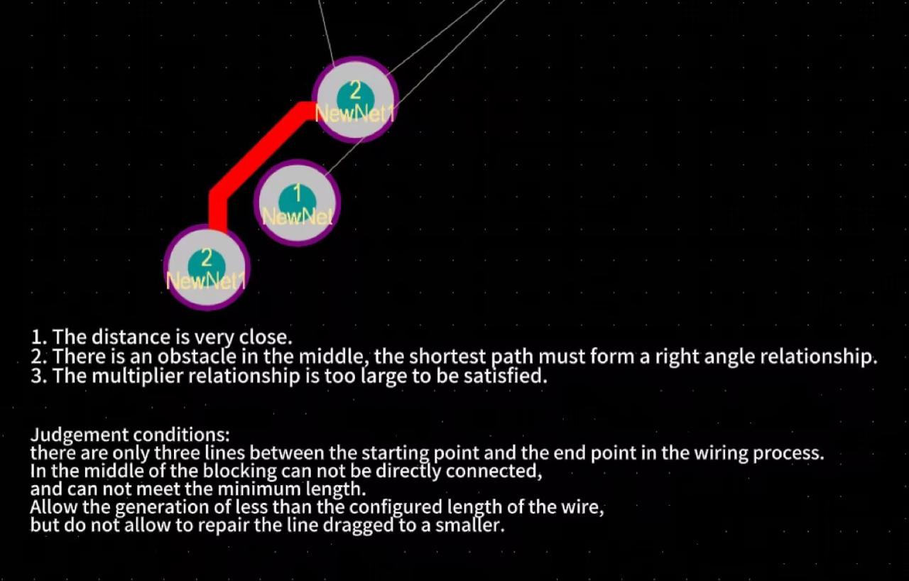
- This configuration applies if there are three consecutive sections of wire with the first and third sections at right angles to each other, and the length of the intermediate section of wire is not less than a multiple of its width*configuration when dragging the wire. It mainly consists of the following scenarios: 2.1
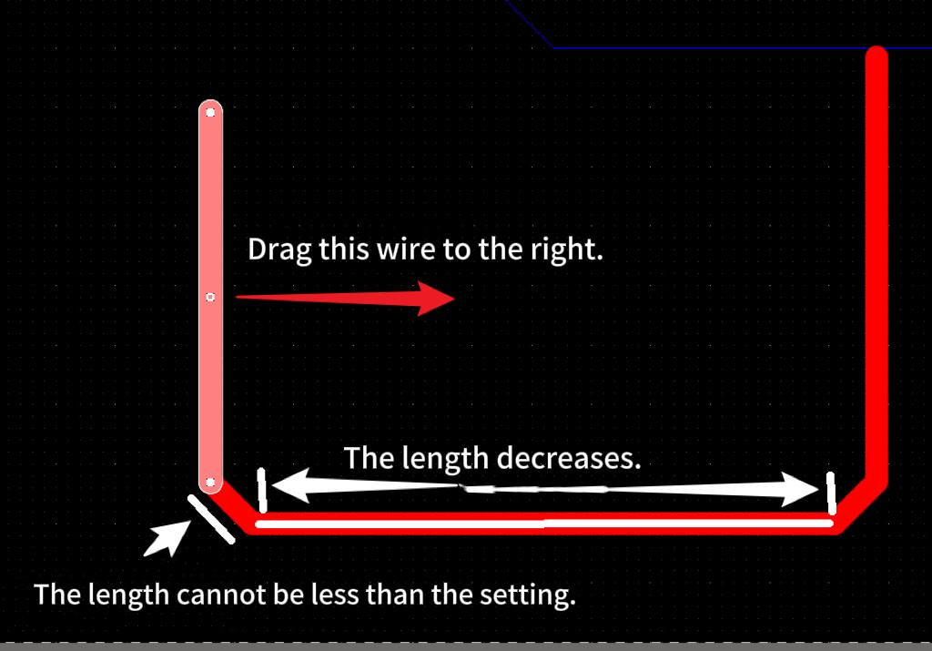
2.2 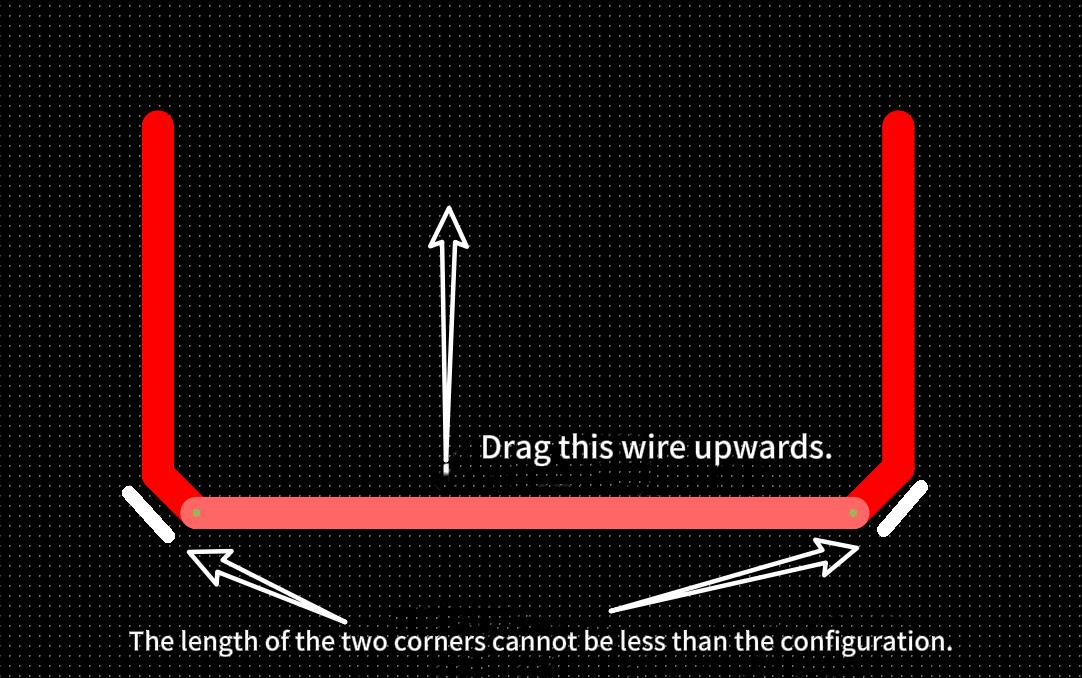
2.3 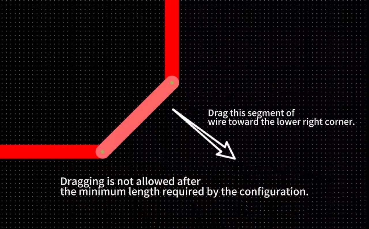
Other notes:This configuration no longer applies to conductors that do not form a 90-degree corner. 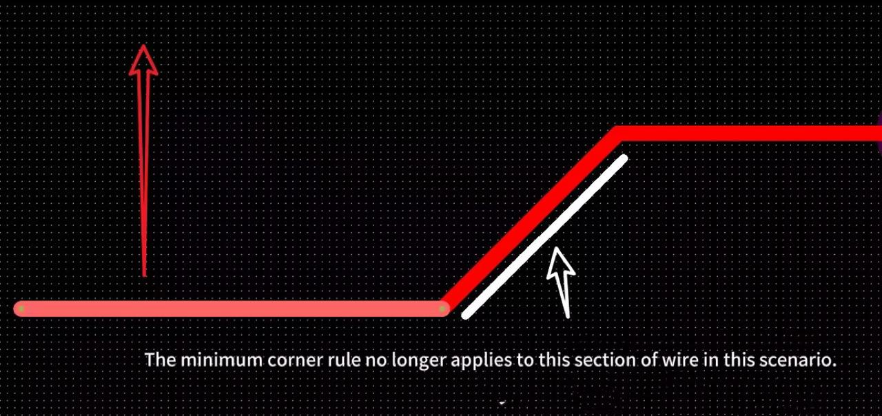
How to add nodes to a line segment?
Details
Select the node in the line and right click on the mouse to manipulate the node. 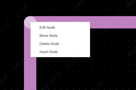
How to set the text to remove the green oil leaking out of the copper skin?
Details
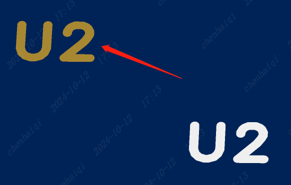
Place the text on the top or bottom layer, and the top soldermask or bottom soldermask layer, respectively, and then overlap them. Finally in 3d preview you can see that the yellow effect means that the copper skin is exposed. 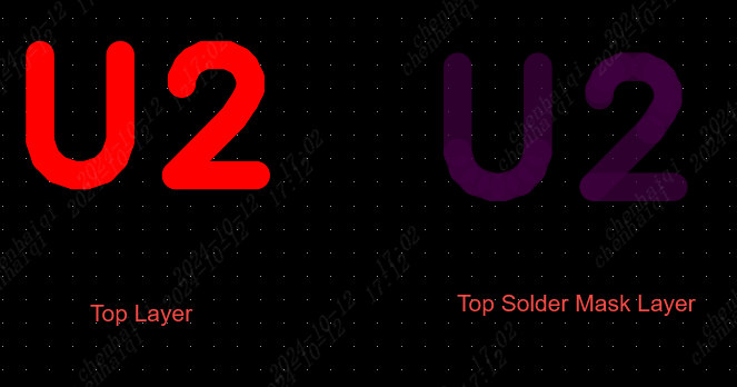
How to merge lines?
Details
Select the lines that need to be closed, click the right mouse button and choose Merge as Closed Lines. 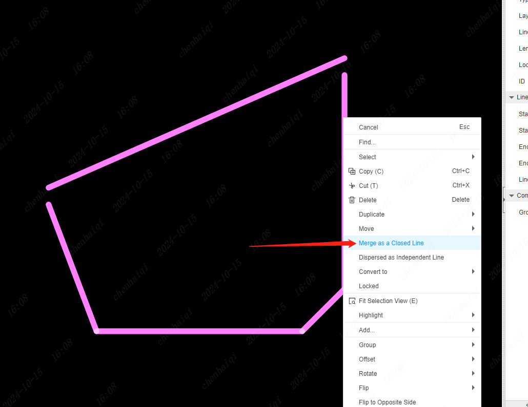
How to set not to check drc when PCB order is placed?
Details
Find ‘pcb-general’ in the Setup Tools on the top menu bar, and uncheck the detection option. 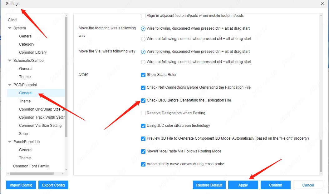
How to import DWG files?
Details
We are sorry that we do not support importing DWG files. Because DWG format is a binary file, it is more complicated, at present our team does not have the energy to study this problem, you can try to save as DXF file in CAD software before importing into easyeda.
How to change the cross cursor setting of the schematic/PCB canvas?
Details
The size of the Cross Cursor can be set in the Settings tool on the top menu bar.It is also possible to set whether the cross cursor needs to be displayed continuously. 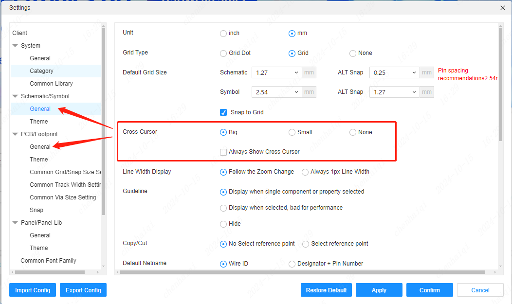
How can PlaneZone layer be modified to Signal layer?
Details
It can be modified in the Layer Manager. 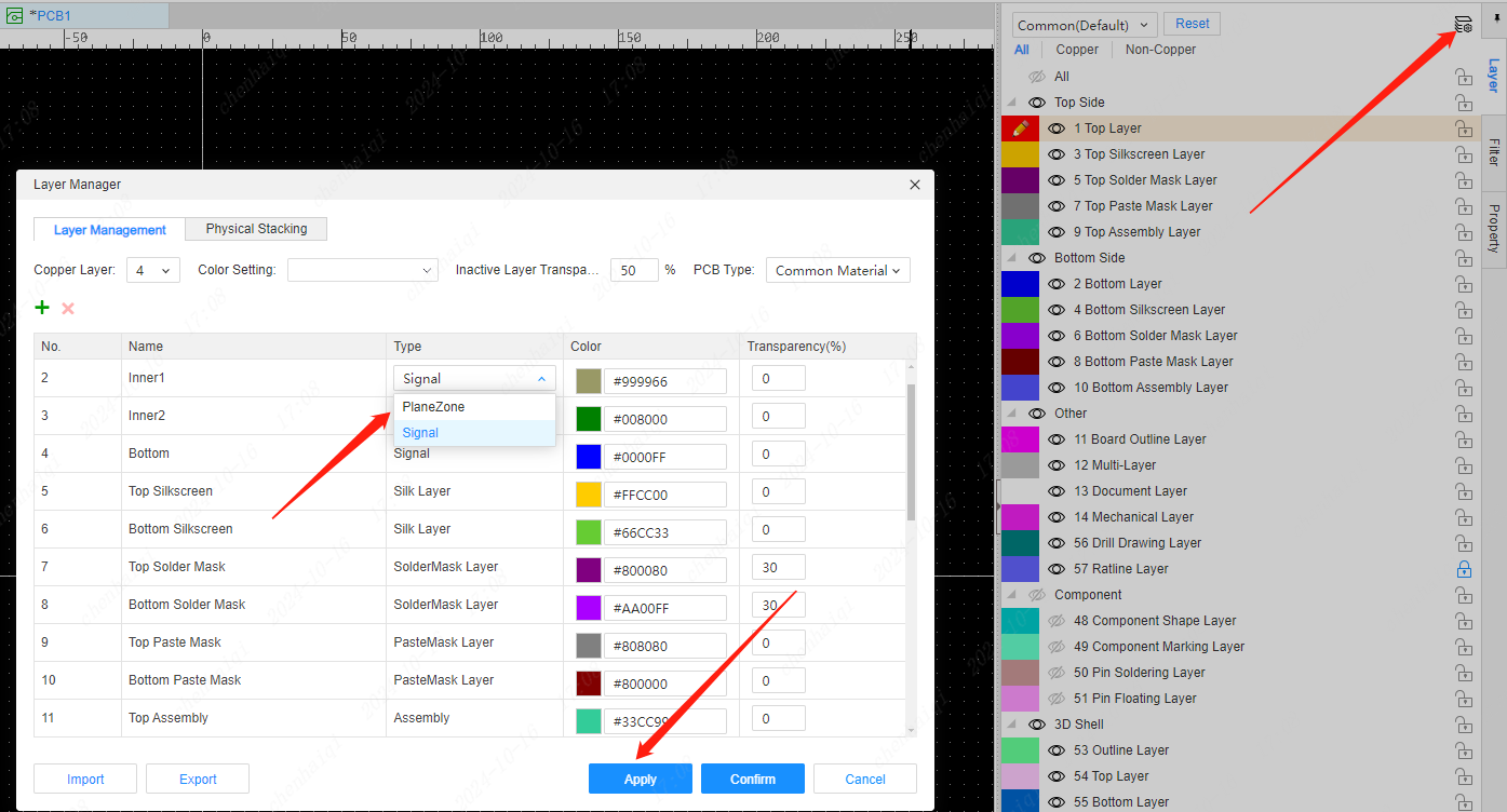
How to use the Reset ID function?
Details
It can be found in the top menu bar of the schematic and PCB.When both the schematic and PCB are reset ID and then clicked on Import Update, the PCB update will not change position. 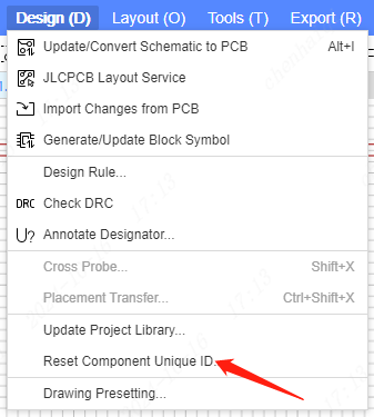
How to set the layer window at the bottom to show and hide?
Details
Top menu bar - View - Windows - Layer Bar 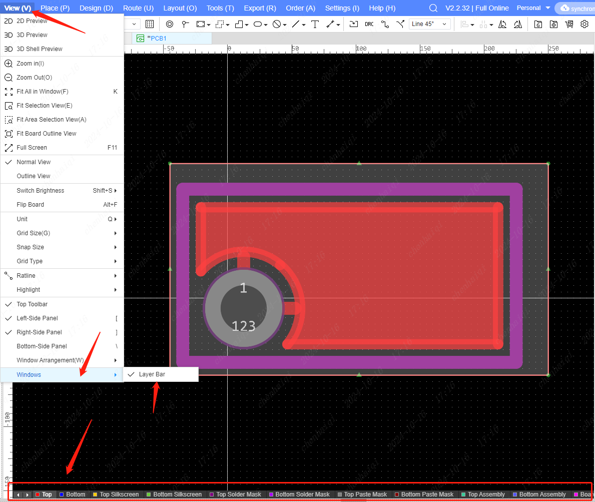
How to display teardrops?
Details
Turn on Show Teardrops inside the right filter bar. 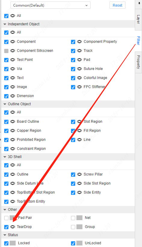
How does PCB customise the checking of DRC design rules?
Details
This tool can be found in the top menu bar. 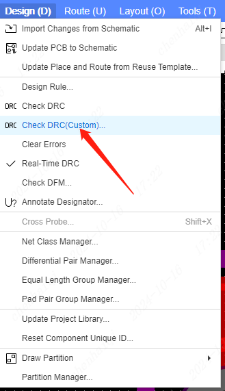
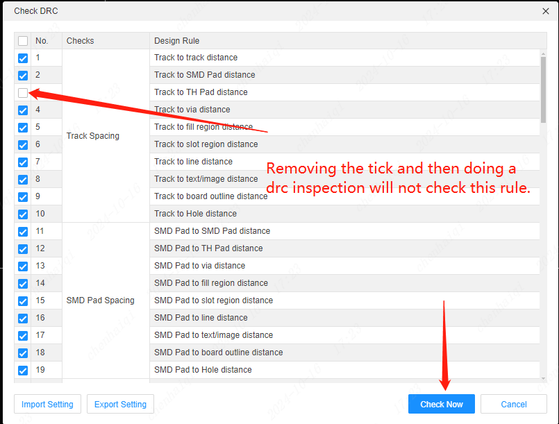
How to remove unwanted solder paste layers?
Details
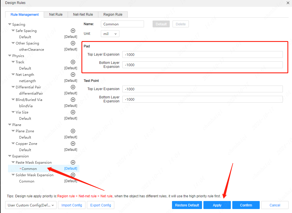
How to remove unwanted solder paste layer in easyeda, here are two methods: 1.select the pad in PCB, set Solder Mask Expansion for the pad.Set the value of Solder Mask Expansion to Custom, and set the value to -1000. When it is 0, the solder resist shape is as big as the pad shape, and when it is negative, it is smaller than the pad shape. 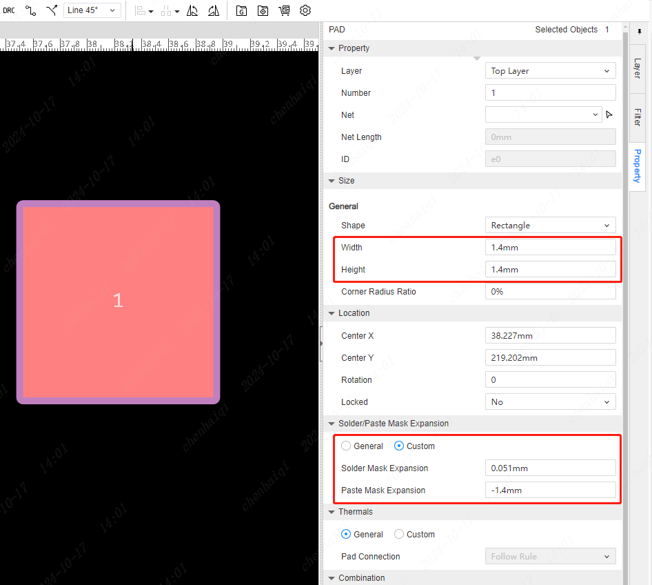 If you don't want to set them one by one, you can set them directly inside the design rule. pad's Solder Mask Expansion property is by default a generic type (following the rule).
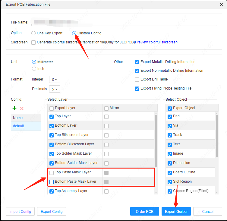
  2.In the export of the Gerber file, select the custom export, do not tick the solder paste layer, note: after ticking will be the entire usual not designed in the solder paste layer will not be exported!!!!
How to set an element's attributes to show or hide by default?
Details
First method: turn the eyes off or on in the right filter panel.  Second method: Set a tick in the Properties panel inside Settings.
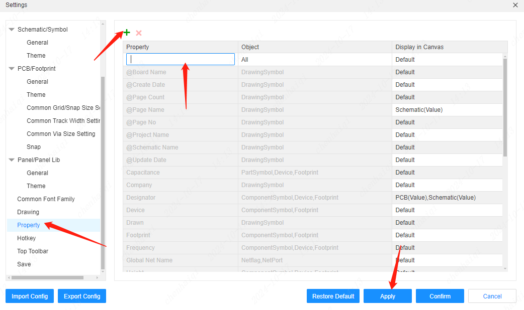
 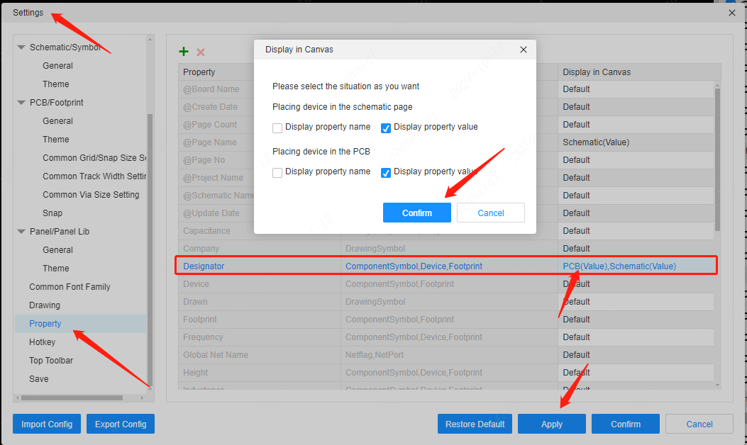 Here you can also add the property settings you want.
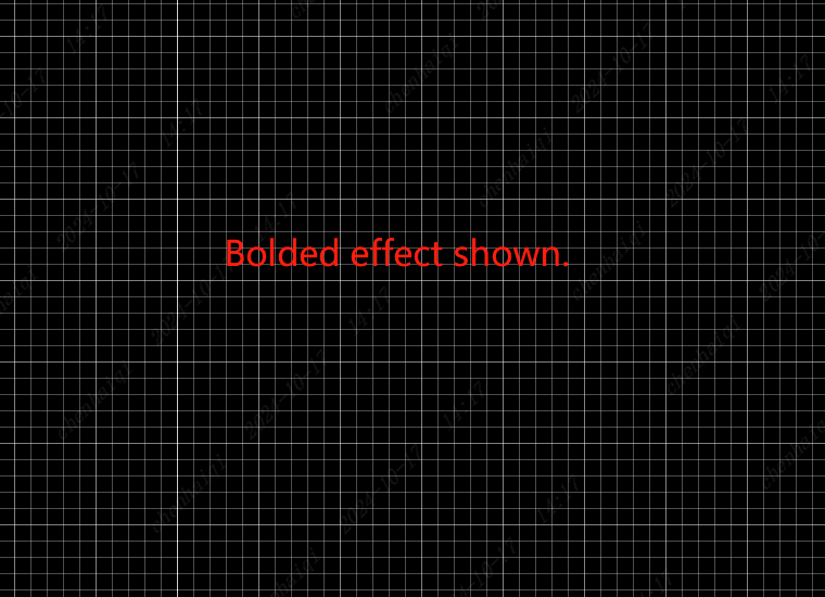
How to thicken the grid of PCB?
Details
Tick inside Settings on the top menu bar. 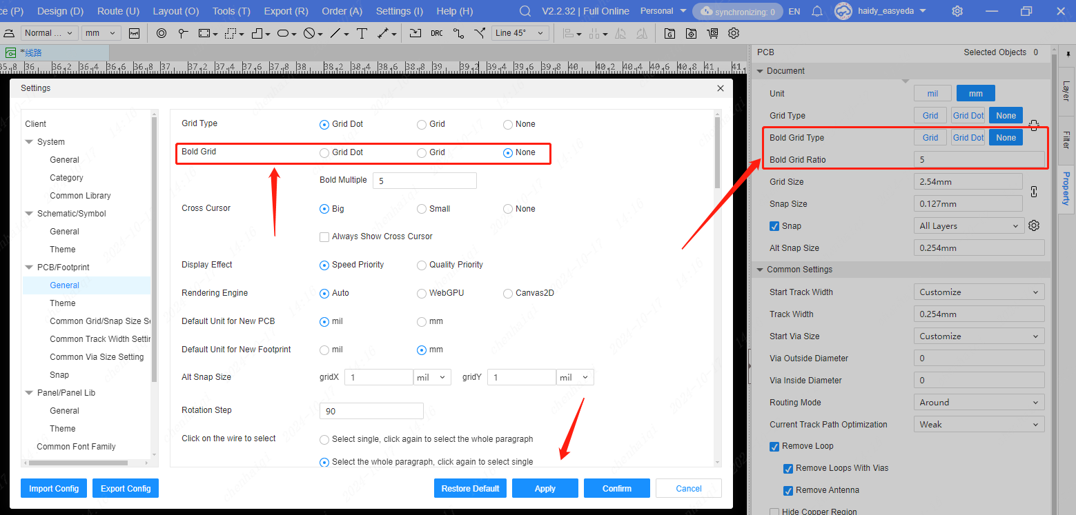
How does the Delete Object function work?
Details
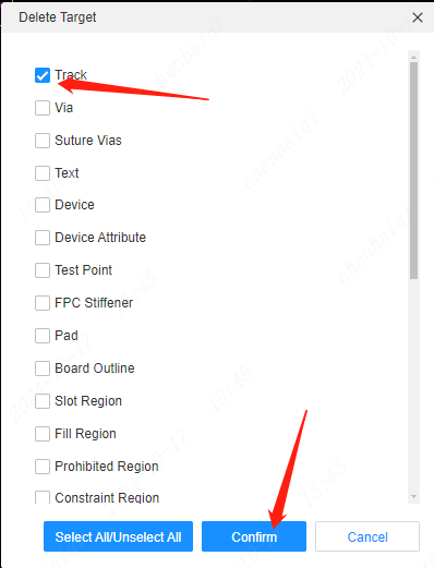
The Delete tool can be found in the top menu bar, where you can choose to delete all (meaning all elements in the pcb) or a specific object. 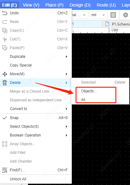
How to open Dynamic Input Box?
Details
It can be found inside the Settings tool on the top menu bar. 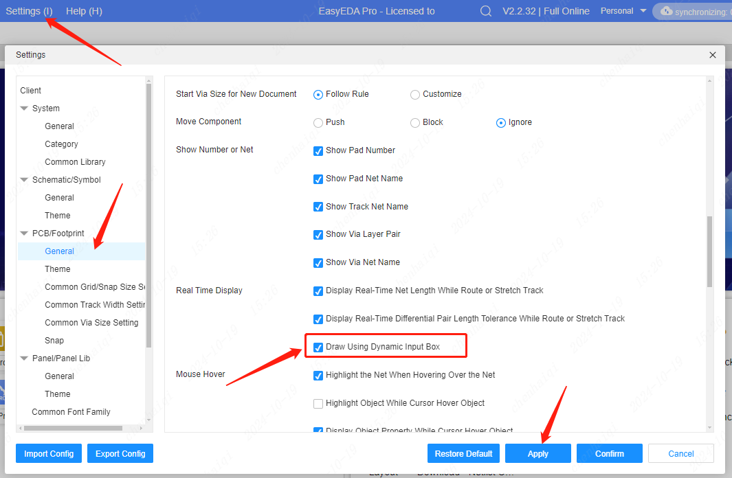
How do I quickly align the top wiring with the bottom wiring?
Details
After finding the selected wire, right click on the menu to have the flip-flop function. 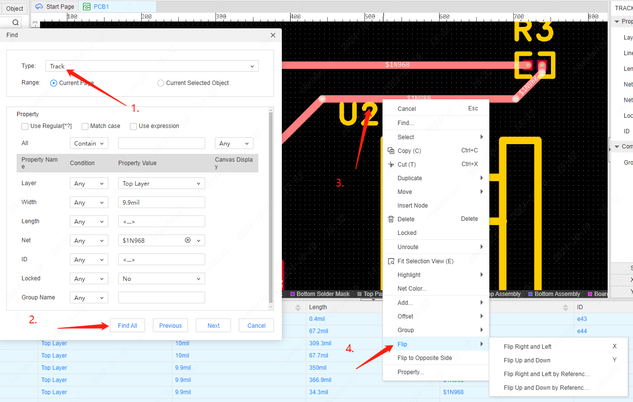
How to set "Align in adjacent footprint/pads when mobile footprint/pads"?
Details
It can be found inside the Settings tool on the top menu bar. 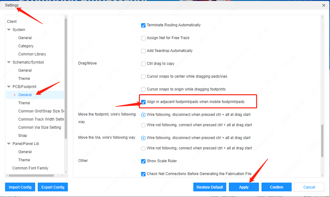
How to bind 3d models?
Details
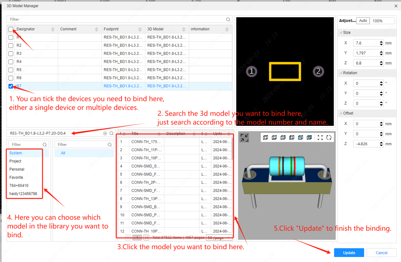
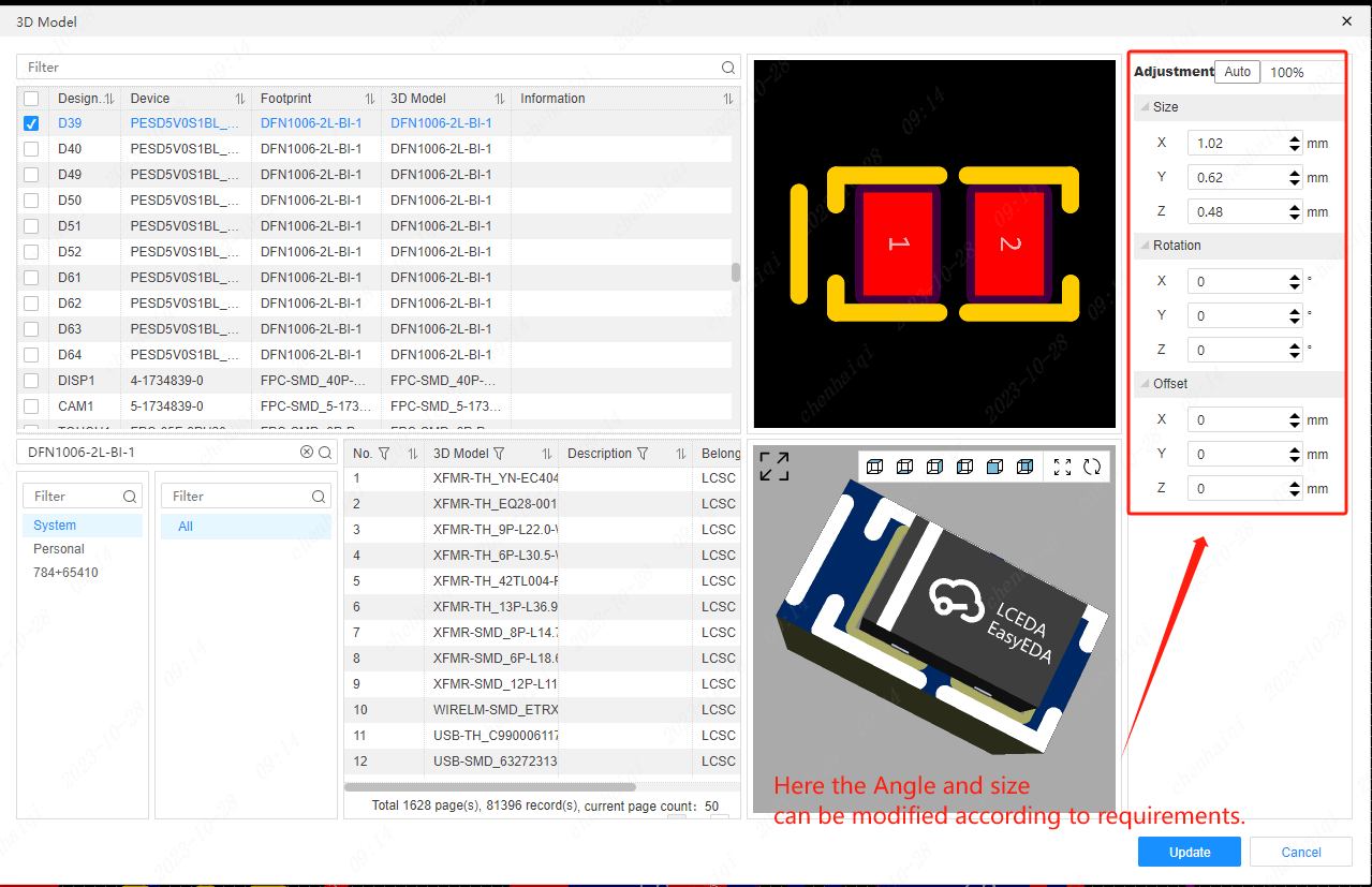
In the top menu bar of PCB interface, there is the function of 3d model manager, which can achieve the function of batch binding 3d model and modifying 3d model. 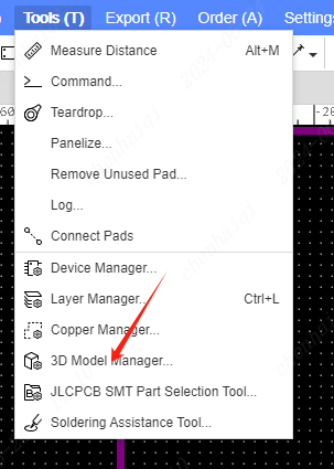 Then you can see all the components you are using on the manager. Including clicking on them, you can clearly see that they are bound to the 3d model. If they are not bound to a 3d model, you can search for their 3d model name in the search bar below and bind them. You can also use the toolbar on the right to make adjustments to the appearance as well as the position of the 3d model. Finally when there are multiple identical components, you can batch tick them to bind a 3d model at the same time in the tick box above.
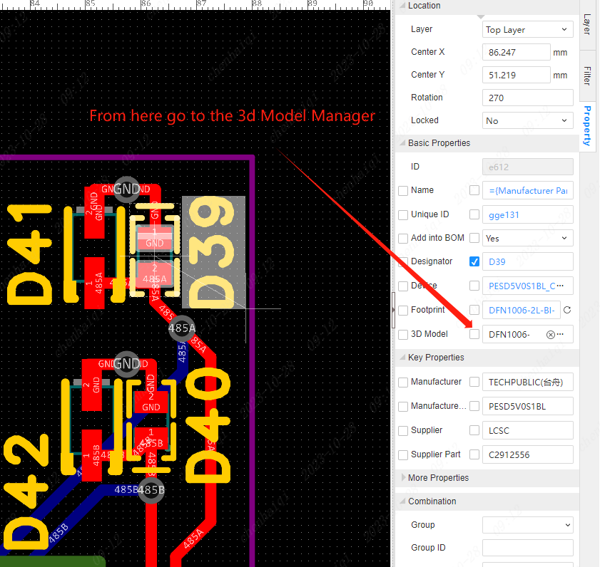
How can 3D models be resized, offset and rotated?
Details
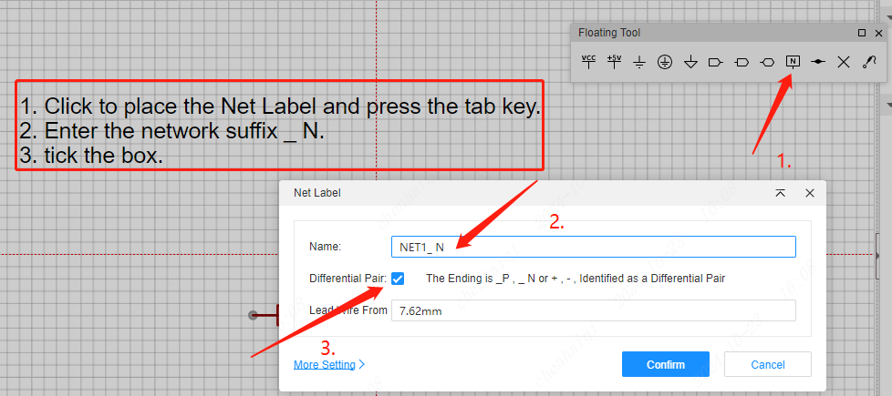
How to name schematic network labels in the form of differential pairs?
Details

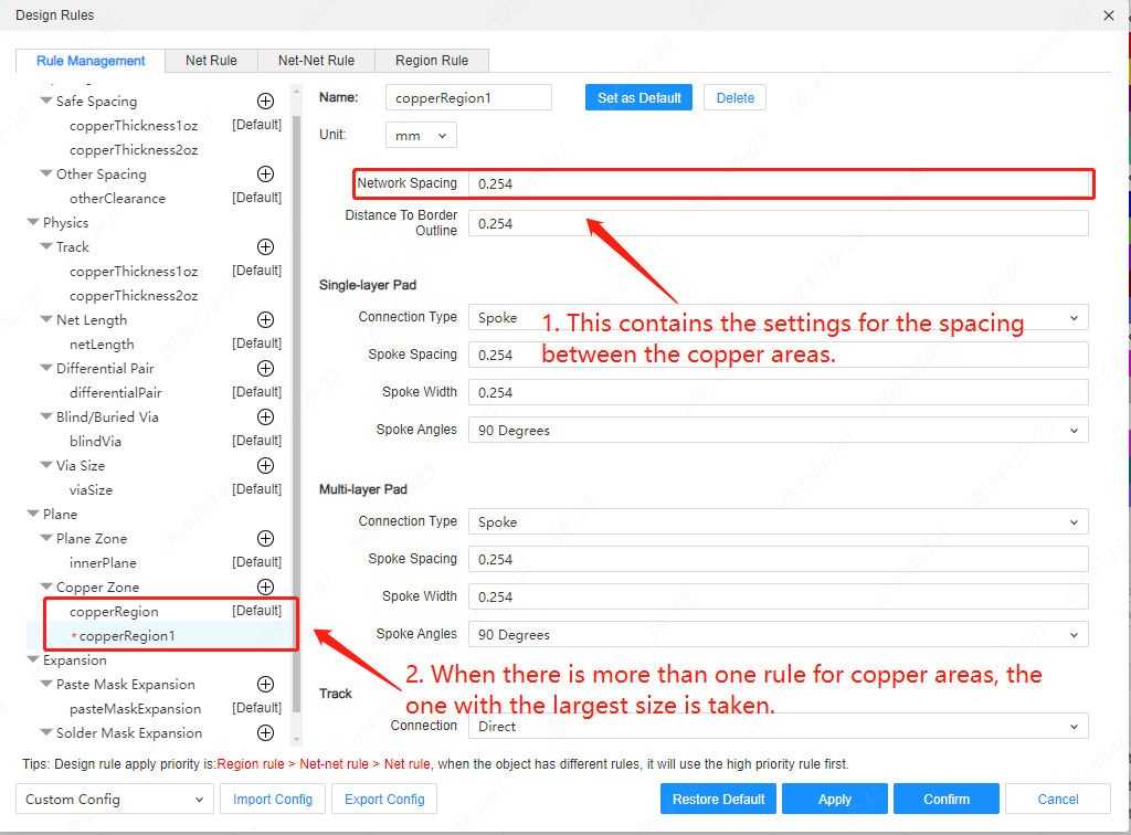
How is the spacing between each copper area set?
Details
How does a PCB automatically generate a network when there is no schematic?
Details
In the top menu bar, under Setup Tools, find PCB's General Settings and tick the ‘Assign Net for Free Track’ option. 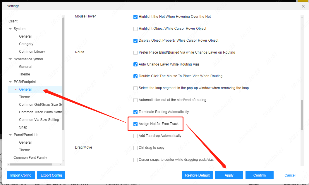
How to hide a particular network ratline?
Details
In the Project Design panel on the left, find ratline in the Network column.You can also use the shortcut keys: tap the network you want to hide and press Ctrl+R to hide or show it. 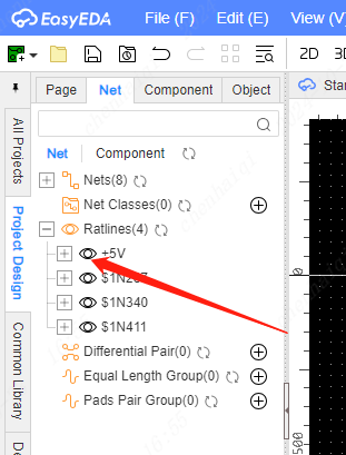
How do I set an element to move in the centre?
Details
Select the component and press the hotkey ‘M’ or click the right mouse button to select it. 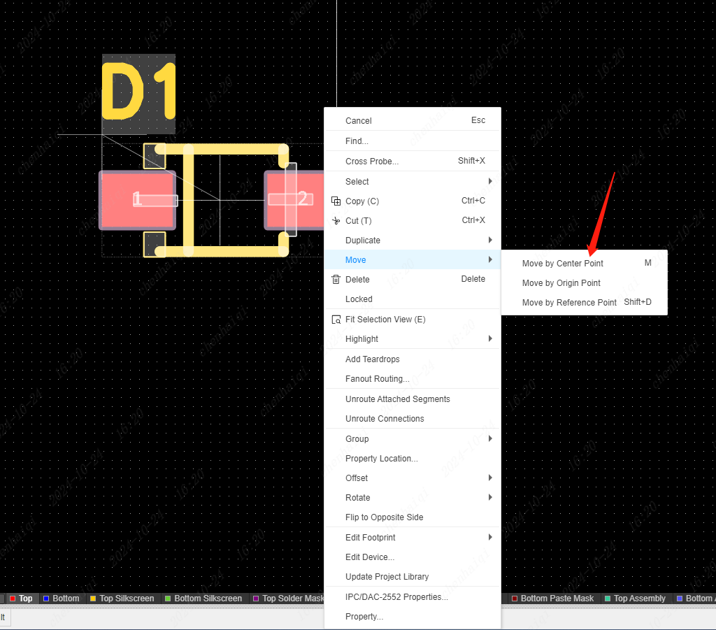
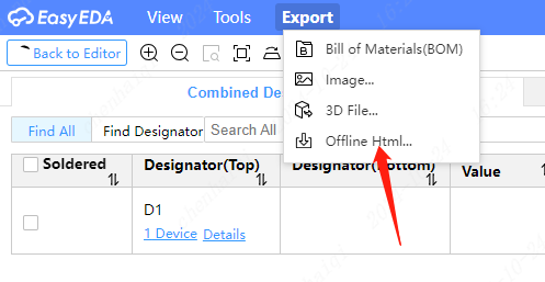
How to export offline html file?
Details
Top toolbar: Tools - Soldering Assistance Tool - Export - Offline html 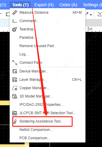
How to place the shaped pads?
Details
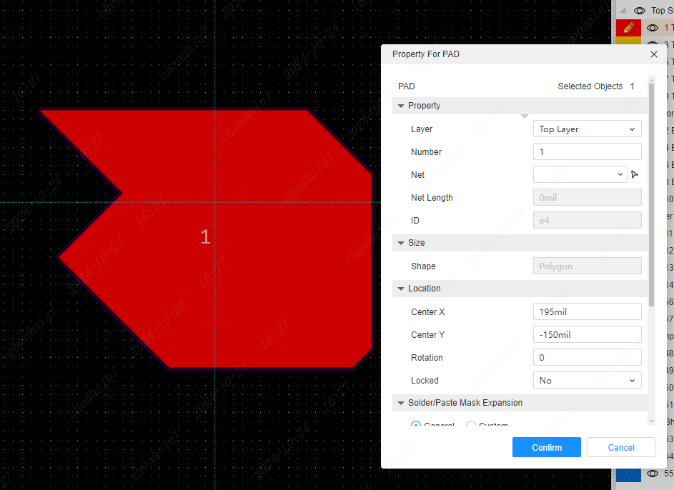
Top Menu Bar - Placement - Shaped Pad 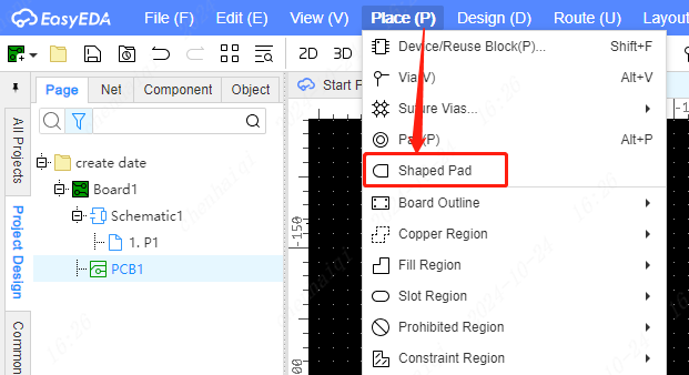 After placement you can enter the property settings you want.
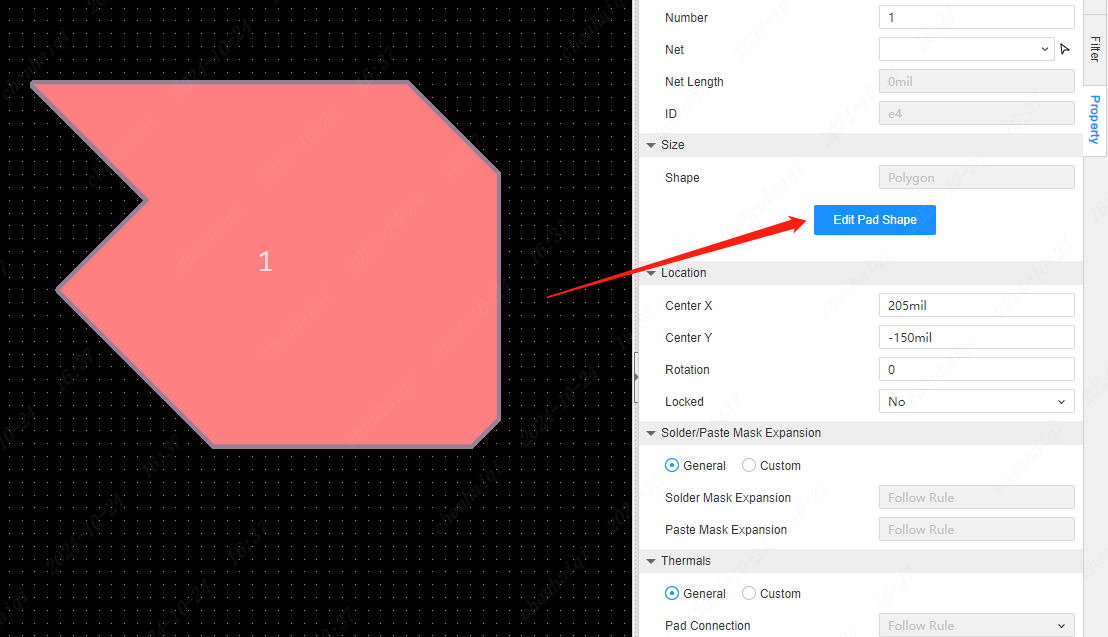
  Clicking on the pad also gives you the option to continue editing the shape in the Properties column on the right.
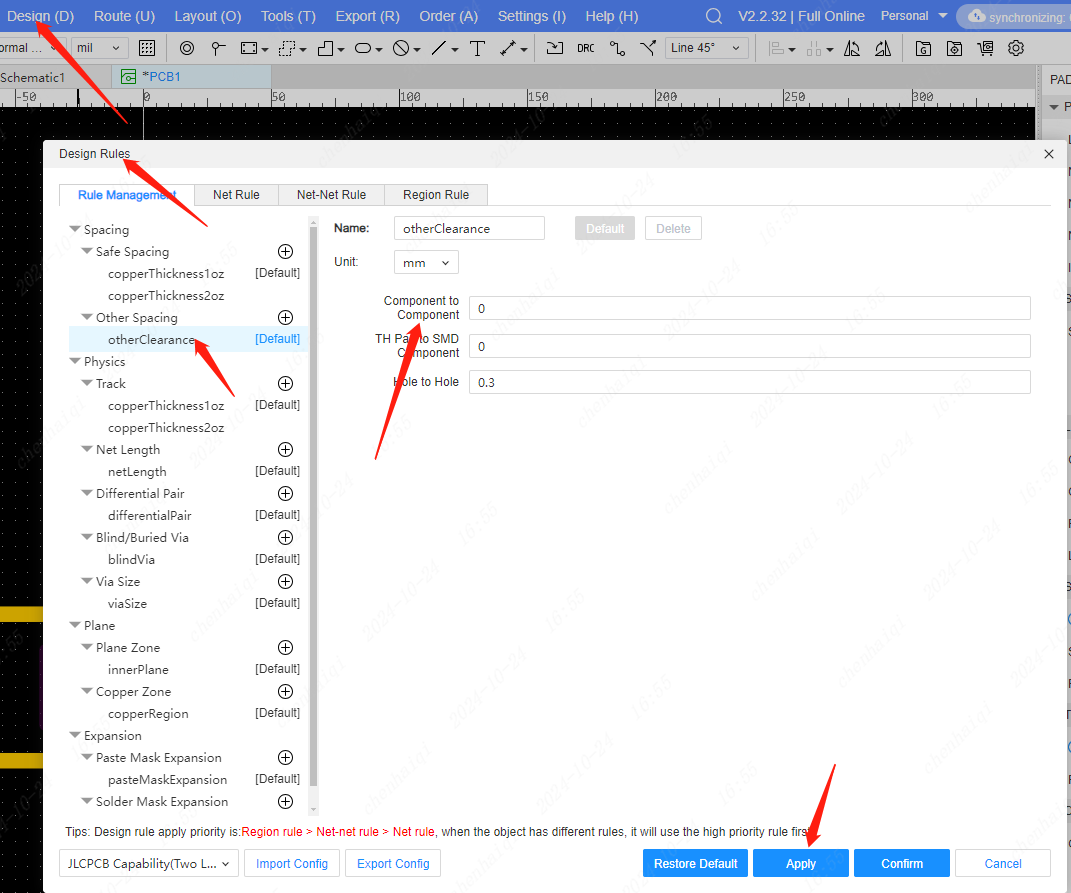
How to set the device-to-device DRC spacing rule to report an error?
Details
How to mirror the footprint?
Details
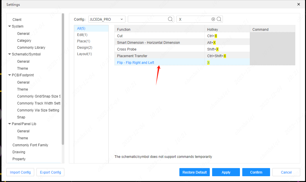
The first method: drag the footprint, press X,Y shortcut key, will pop up whether the mirror flip, the point can be determined. If it doesn't work, just set the shortcut. 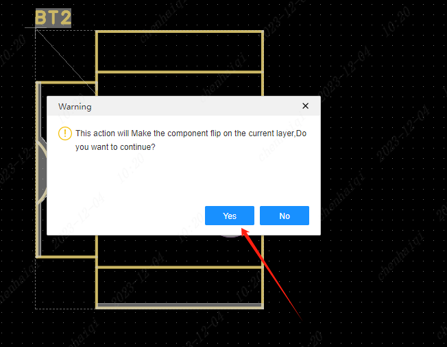
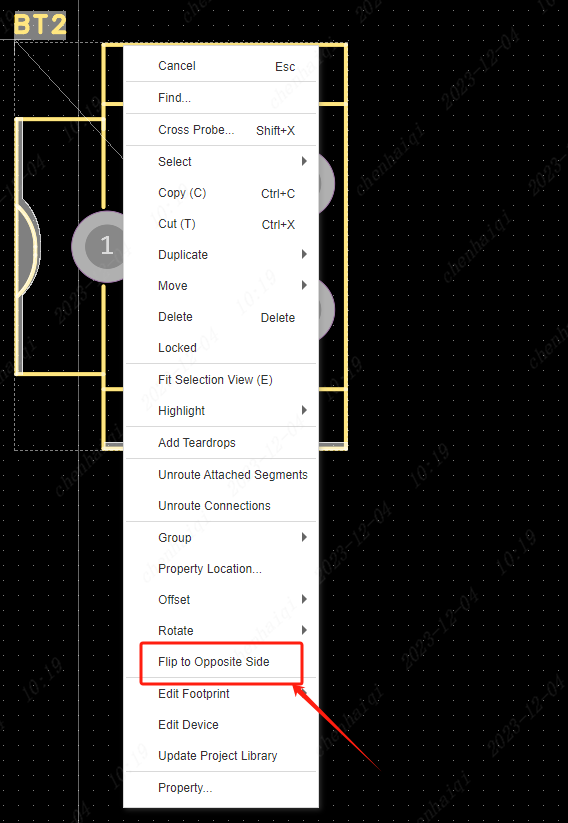
 Second way: select the component, then right click and select Flip.
What if the copper area is not displayed after placing the copper area?
Details
There are several reasons:
pcb needs to have drawn board outline and check if the board outline has been closed.
whether there are other elements with the same network within the copper region range.
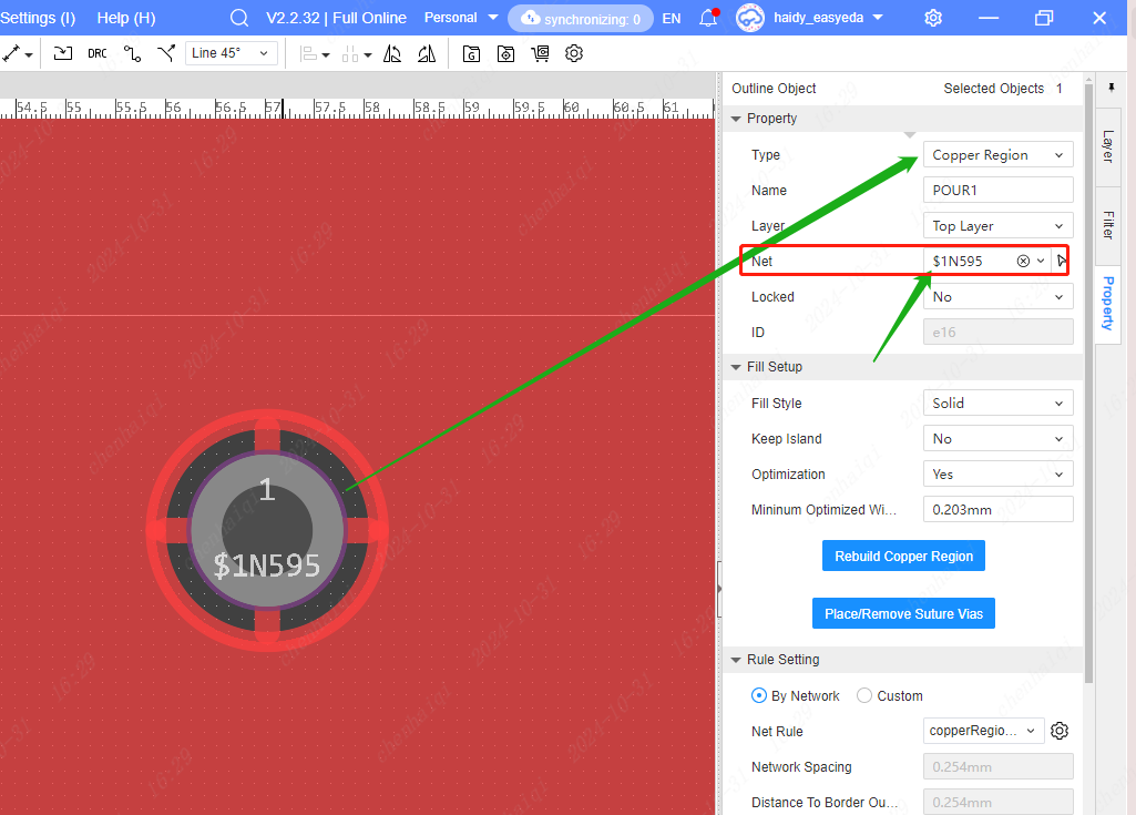
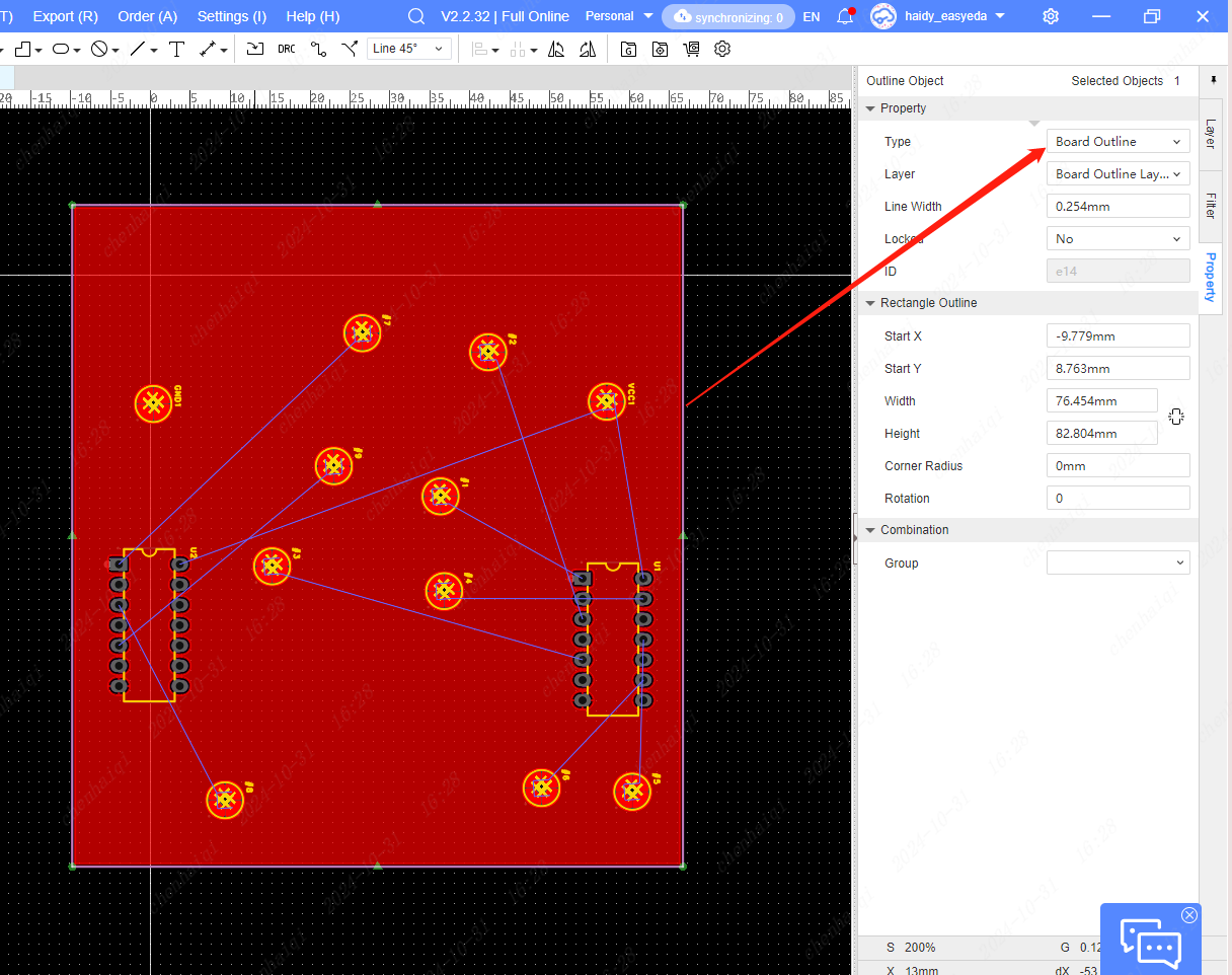
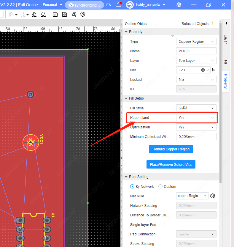
If you want to pcb to have a separate network, you can click on the wireframe of the pcb, and change the attribute ‘’keep islands‘’ to ‘’yes‘’ in the property panel on the right.
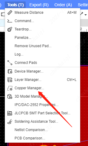
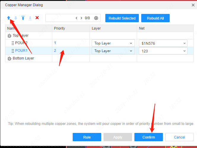
In the Copper Manager in the top menu bar, move the small areas of copper region that are not shown to the top of the large copper region .
How to change the thickness of the pcb?
Details
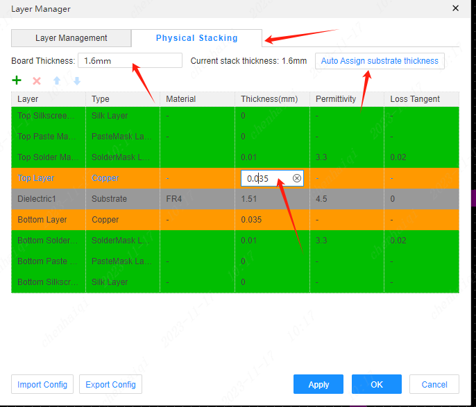
Step 1: Go to Layer Manager. 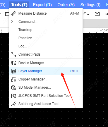 Step 2: Go to Physical Stacking to customize the thickness. You can choose to change the thickness of the entire board and divide it evenly, or double-click to change the thickness of a single board.
How can I replace one of the components in a finished project without modifying the rest of the layout wiring?
Details
When we finished a project, suddenly want to change one of the components, but do not want to move the other layout of the wiring how to do? First of all, you can not replace the schematic directly after the completion of the click on the update pcb, which will lead to pcb layout wiring disrupted to start again. Specific operation please look down: Step 1: first in the schematic diagram to replace the components need to be modified as well as the layout of the wiring, and save. 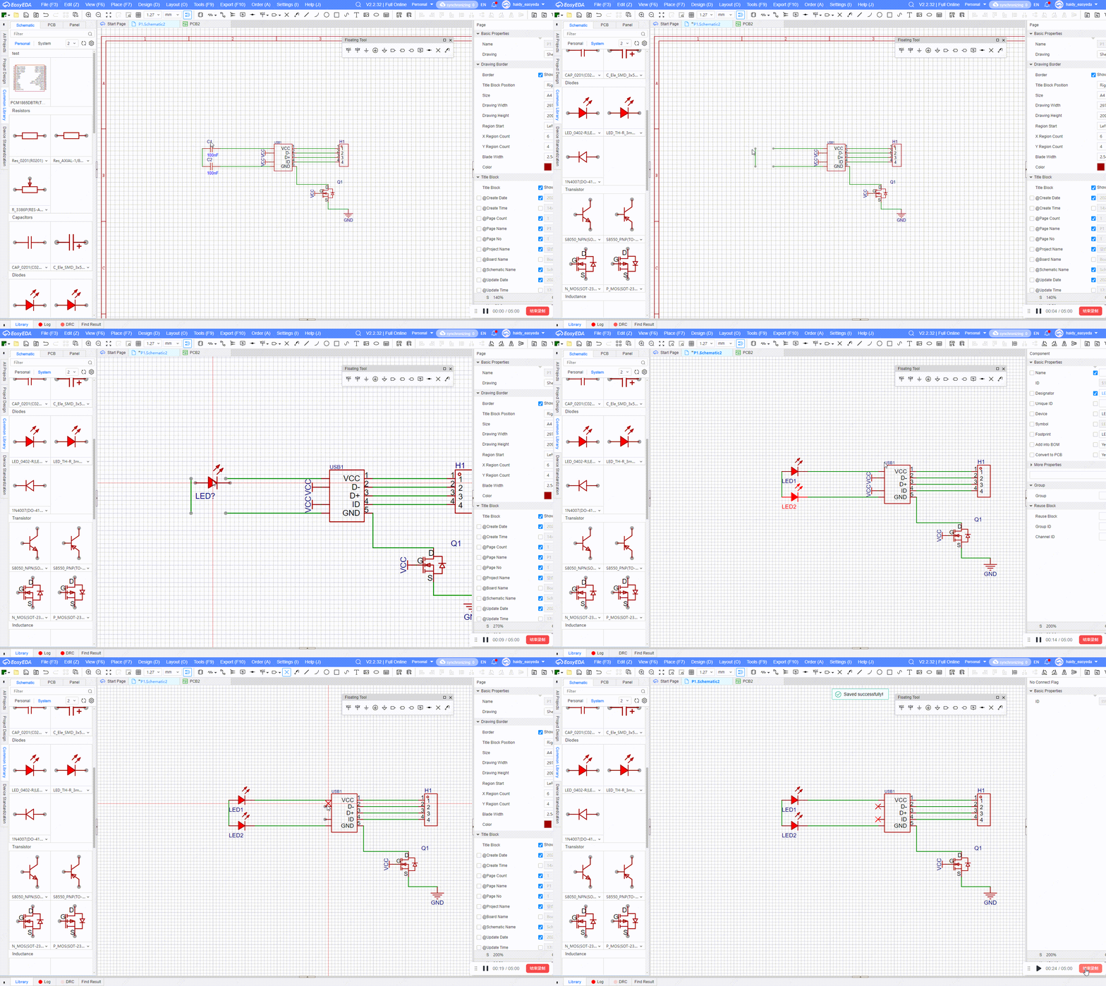 Step 2: Find the Reset Component Unique ID functions in the top menu bar of both the schematic and pcb and click on them respectively.
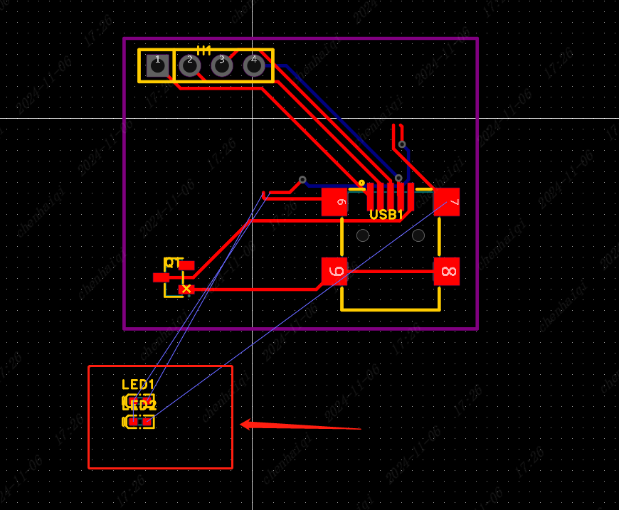
 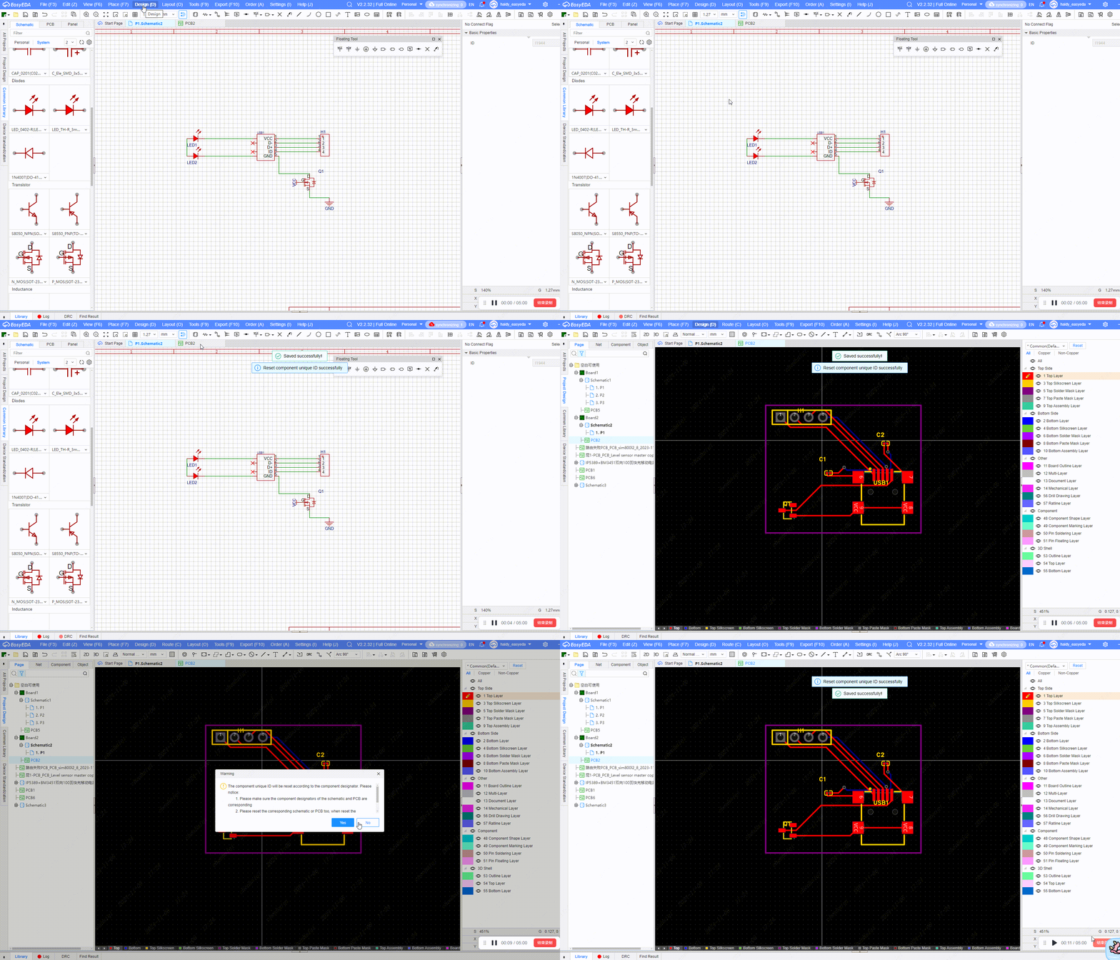 Step 3: Update the pcb again. This time only the replaced components will appear at the bottom, here you need to manually reposition and rewire them a bit, while the other components will not move out of position.
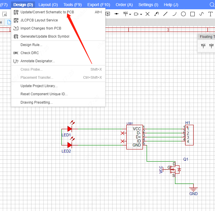
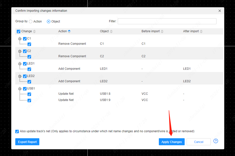
 Second method: Use the Device Manager. The Device Manager is available in the top menu bar to make a selection of components to be replaced.
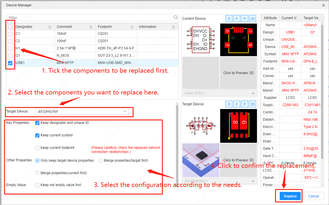 After the schematic replacement, just click on Update PCB in the top menu column once again.
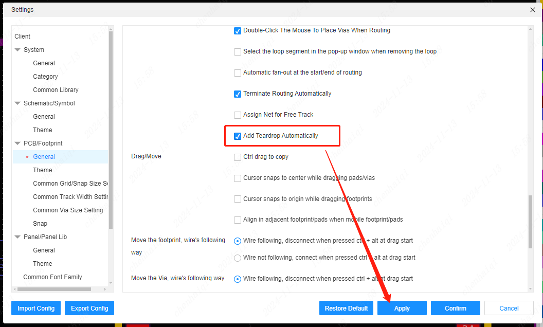
How to set up automatic teardrops for wires?
Details
Find ‘System Settings’ in the settings on the top menu bar and then tick the option to add teardrops automatically in the pcb. 
How to edit the footprint inside the PCB file?
Details
With footprint selected, click the right mouse button and select Edit footprint. Apply only selected components: refers to modifying the currently selected footprint alone. Apply the whole project: means to modify all the footprints of this type on the canvas. 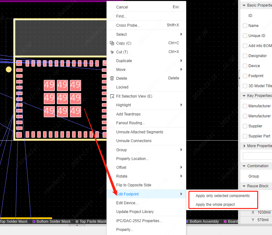
How to batch delete wires on the same network?
Details
Find Network Tools on the left, select the network you want to delete, click on it and after you see all the network wires highlighted, move your mouse over the canvas and click the right mouse button to delete it. 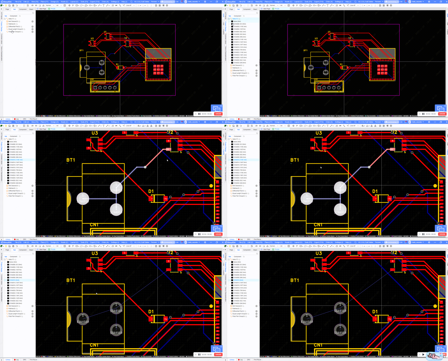
How do I set up individual rotations when rotating devices at the same time?
Details
There are new features in the Pro version for batch rotating devices. You can choose to rotate individual devices or rotate the whole device when you want to rotate them together. 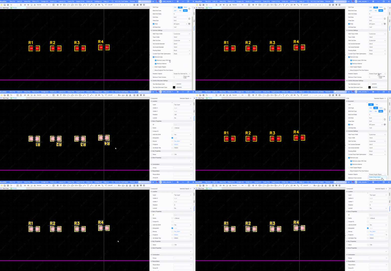
How to make a coil for a spiral?
Details
Helical coils can be obtained by using the Two Points Arc tool in the top menu bar and placing them in consecutive staggered positions. 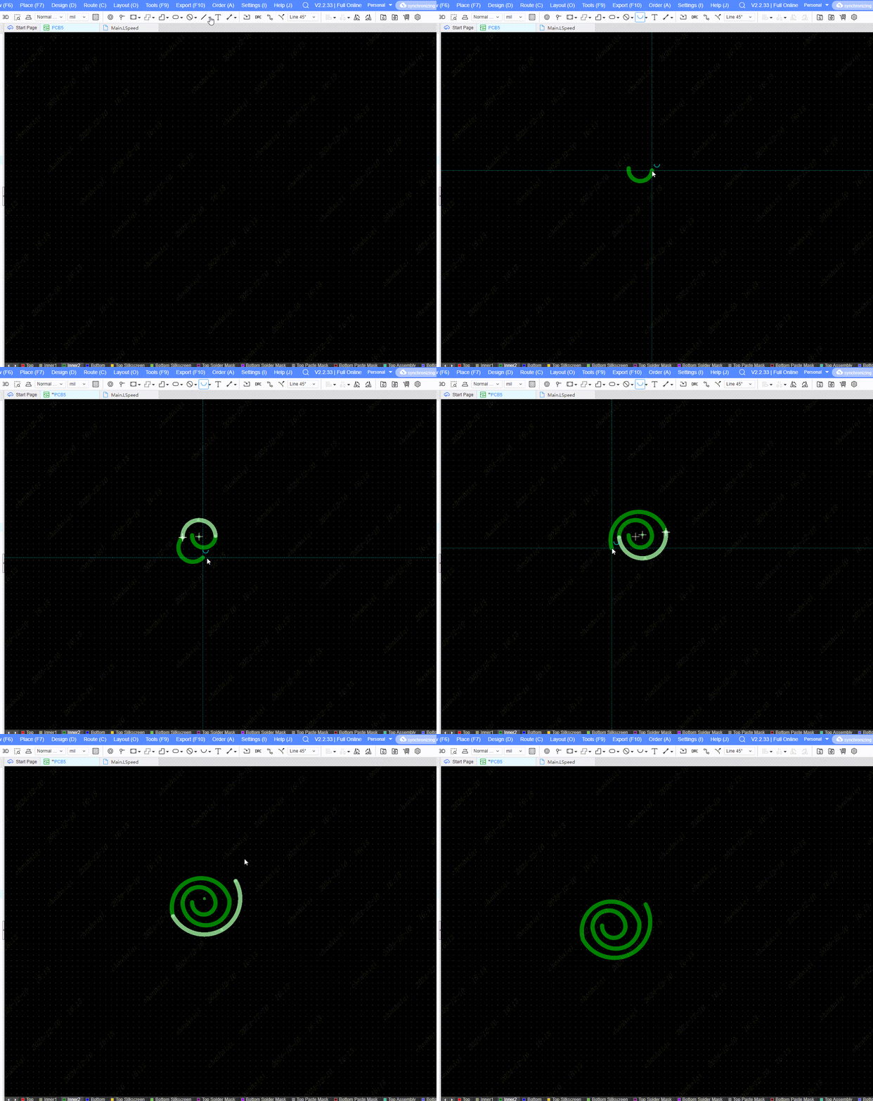
How to draw V-cut panelize by myself?
Details
Step 1: Copy and paste the board with ‘ctrl + c and ctrl + v’. 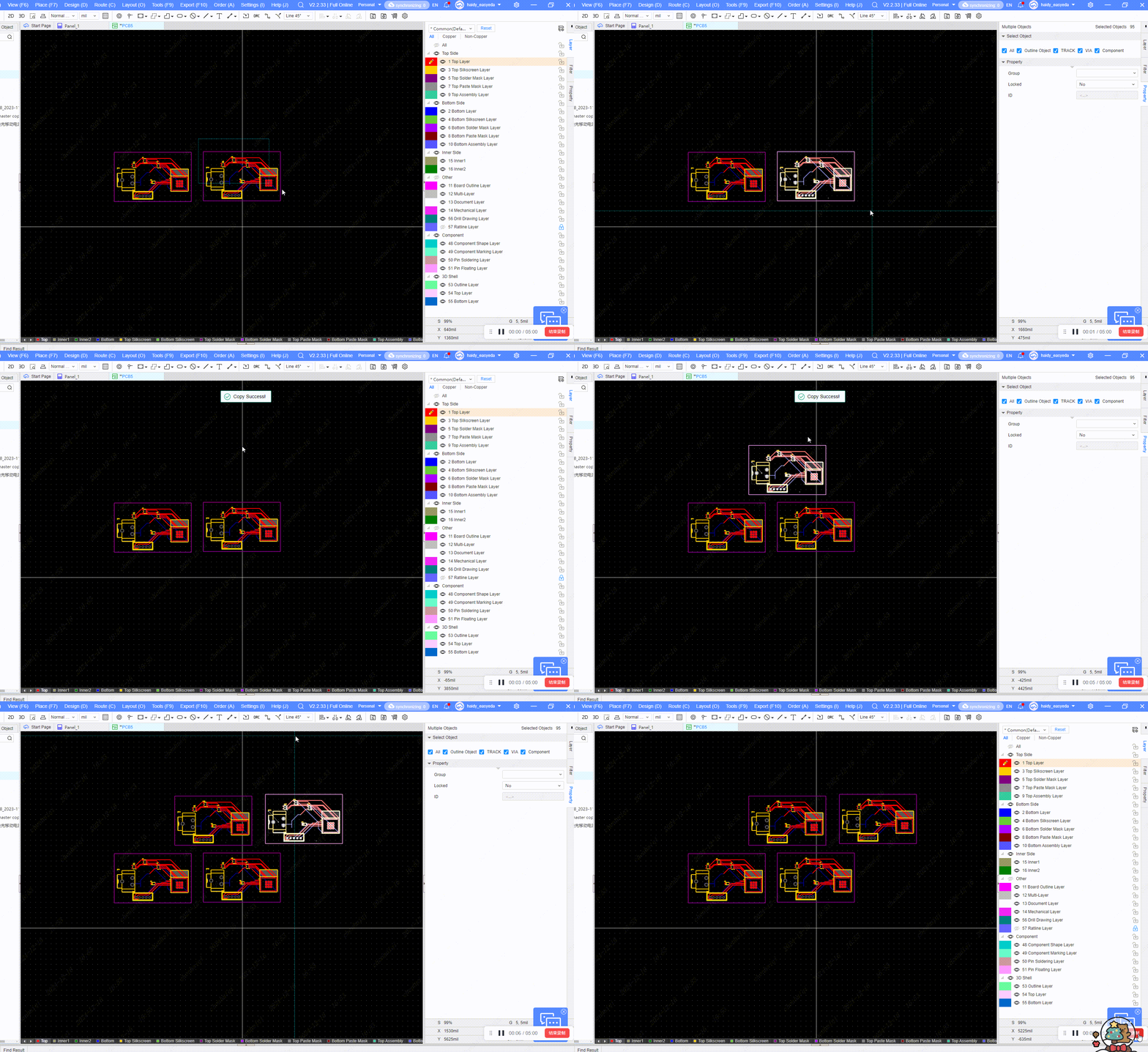
Step 2:Piece them together while aligning their edges. 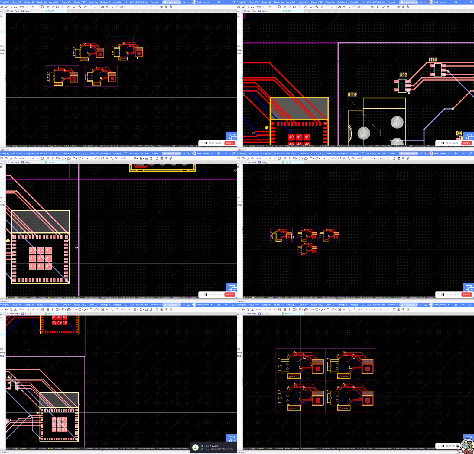 Finally you can add craft edges and mark points as you see fit. The craft edges and v-cut lines are just drawn with a board outline line.
What happens when the pcb turns black?
Details
When you open the pcb after the discovery of the previous drawing of the pcb are all gone can be dealt with in this way: first go to the 3d preview to check whether the board exists, if so, modify the settings inside the engine for 2d mode. This is because the new version of the optimisation, some computers do not support the gpu engine will make the pcb black, just need to change the engine can be, not a big problem. 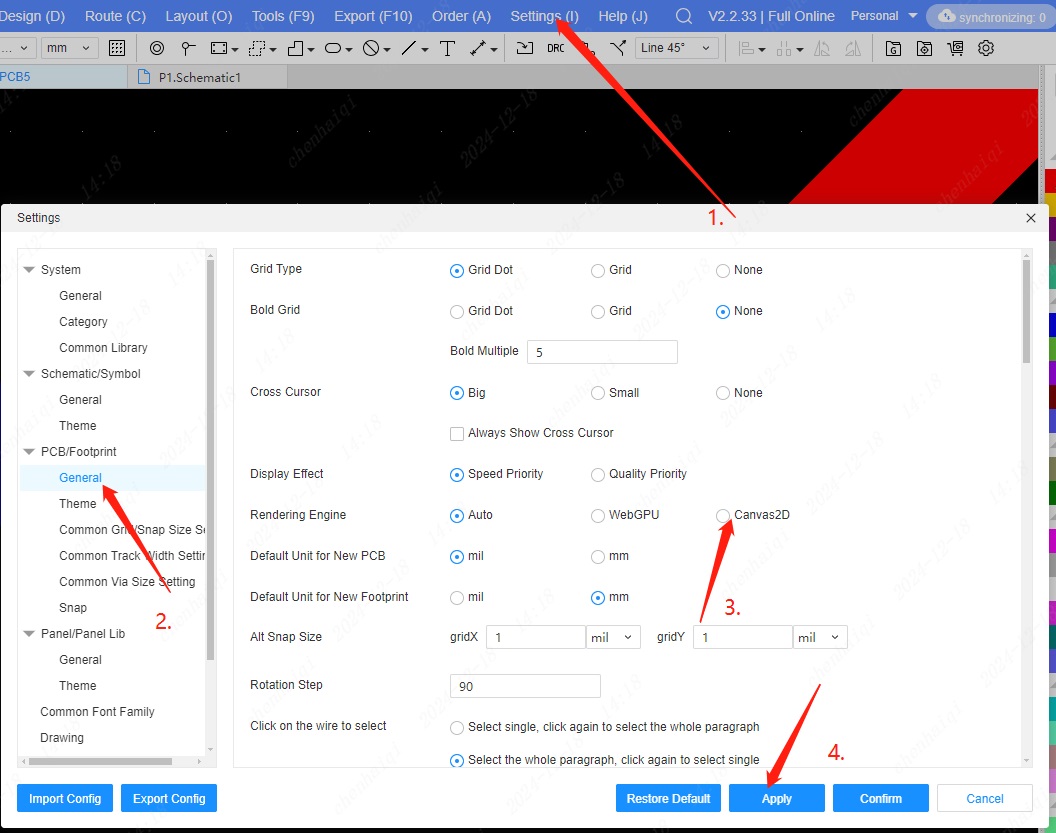
What is the reason when the footprint's profile box is too big or too small?
Details
After we have drawn the footprint, it may appear that the footprint is off-centre and its outline box is too big or too small, what should we do? 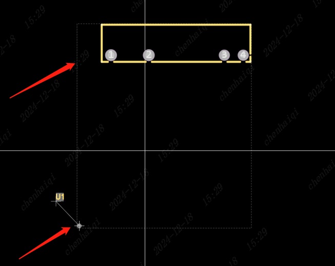 Step 1: Select the device and click the right mouse button to enter the Edit Footprint interface.
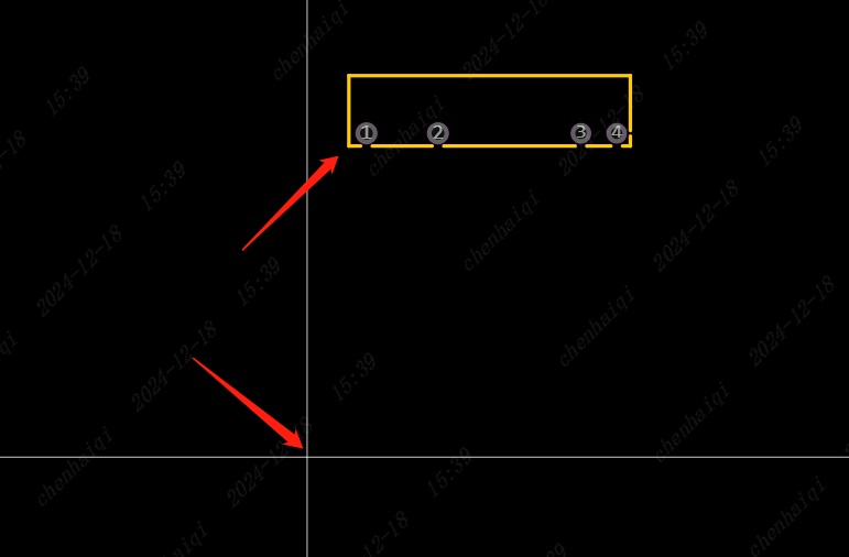
 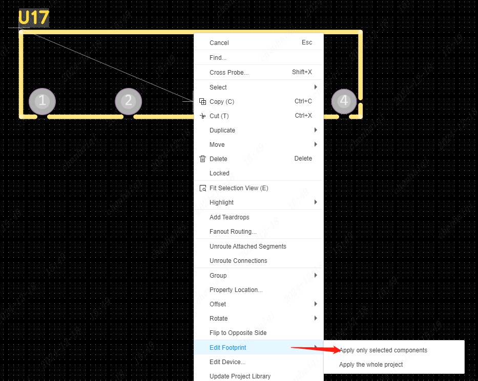 Step 2: Handle the situation with two possibilities. The first possibility: the centre of the drawn package is not within the canvas origin, at this time we need to reposition the origin to the centre of the package and then save the edit.
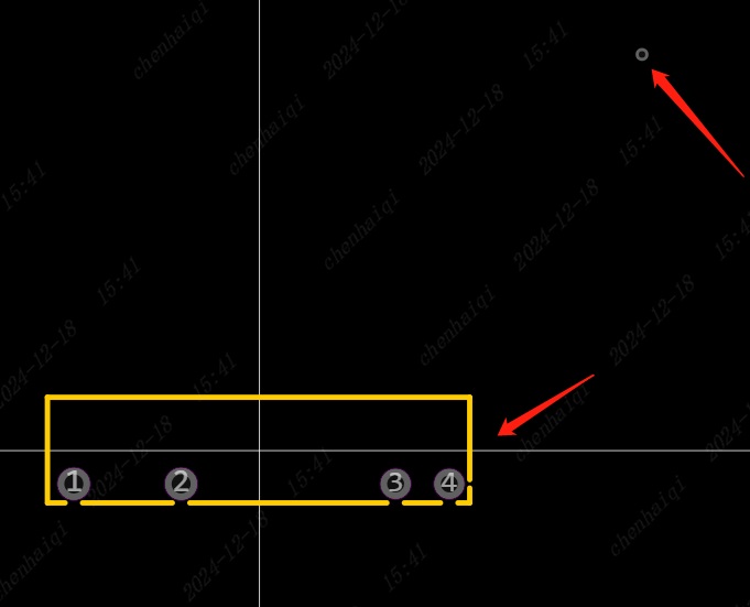
 Second possibility: after entering the Edit Footprints screen check if all the Layers and Filter panels are open and no other elements are hidden, remove the off-centre (redundant) elements and just save them at the end. Because the off-centre elements will also be counted in the footprint design, the shape box will then contain all the designs to be boxed.
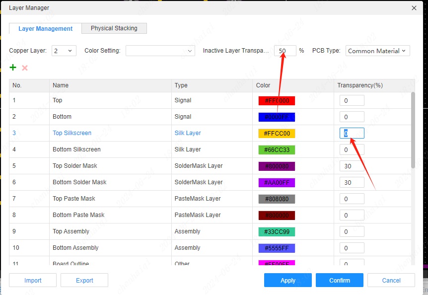
How to change the opacity of a layer?
Details
The layer manager can be accessed from the floating toolbar or the top menu bar.Then you can change transparency。 
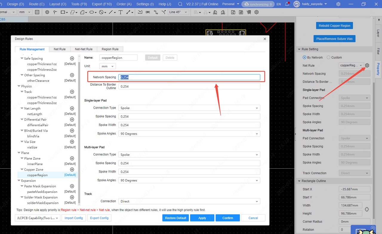
How to quickly modify the spacing between paving copper and elements?
Details
How to quickly modify the spacing between paving copper and elements? When we need to modify the spacing between the copper-laying area and the element after copper-laying, we can do so:
- Select the copper-paved area.
- Click the Copper Design Rules button in the right property bar.
- Modify the Network Spacing. Note: In general, after setting the spacing, the copper paving area will be updated automatically, if the system does not update automatically, you can use the shortcut key ‘shift + b’ to rebuild the copper paving, this step can prevent the subsequent board errors.
How to use Multiple Routing?
Details
This feature is a new feature of the professional version, which can realize the simultaneous routing of multiple lines, making the design process faster and more convenient. 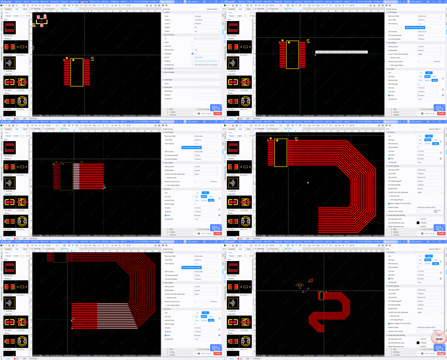
How to choose to display or not display the network name and pad number in PCB?
Details
You can check this option in the settings on the top menu bar. 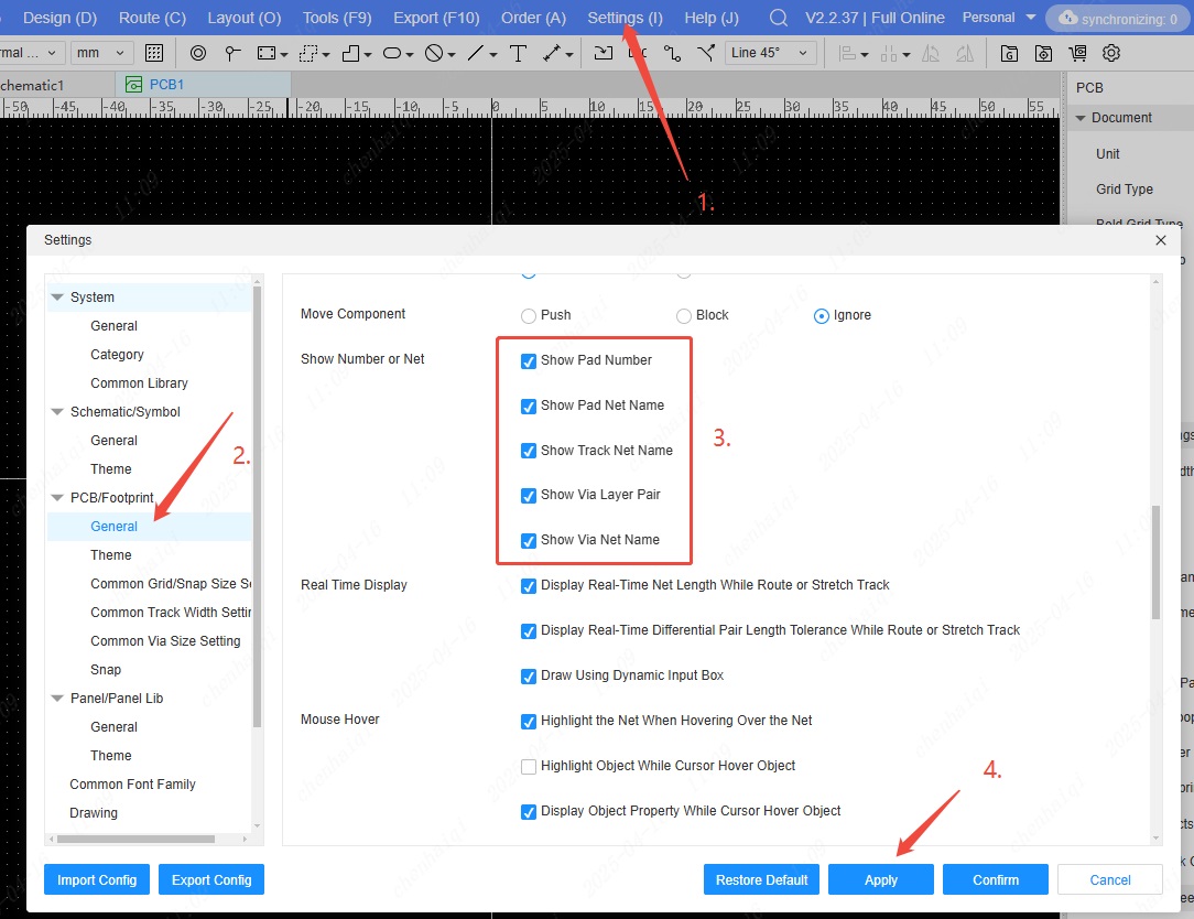
How to remove a loop?
Details
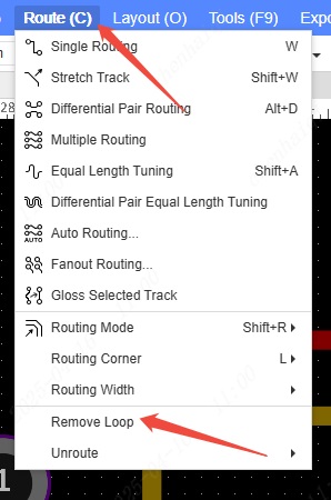
When we need to implement overlapping line design, we can turn off the Remove Loop function in the top menu bar. 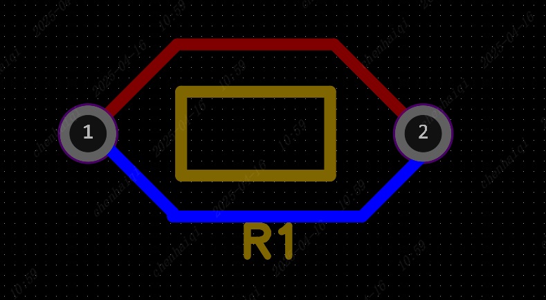
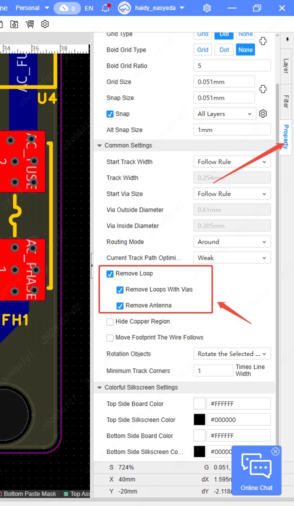
 You can also set this function in the property bar on the right side of the PCB interface.
Why is the teardrop adding unsuccessful?
Details
The main reasons may be that the wire cannot be added:
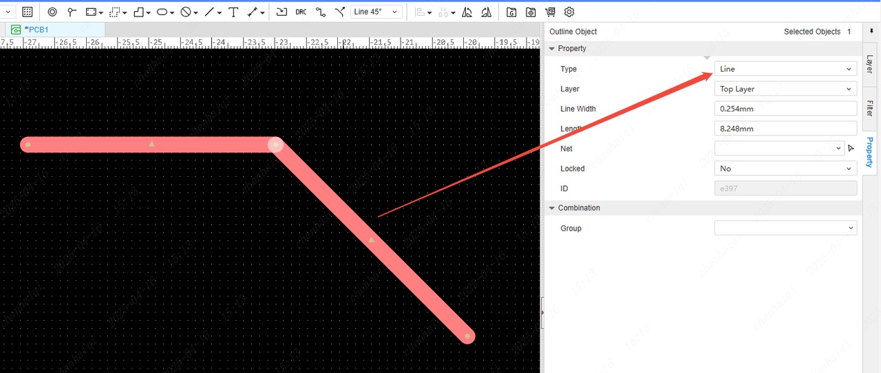
The object added is not a wire but a line, because the line does not support the addition of teardrops.
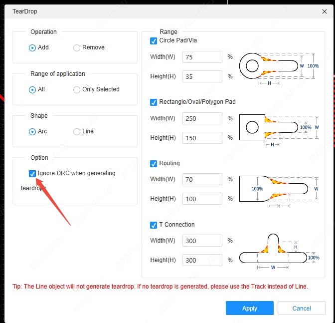
DRC reports an error and cannot add teardrops. You can choose to ignore DRC in the settings.
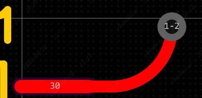
The wire is not connected properly.
The wire is too short and the distance is not enough to add the teardrop area.

Arc wires do not support teardrops.
How to turn on/off the scale ruler of PCB?
Details
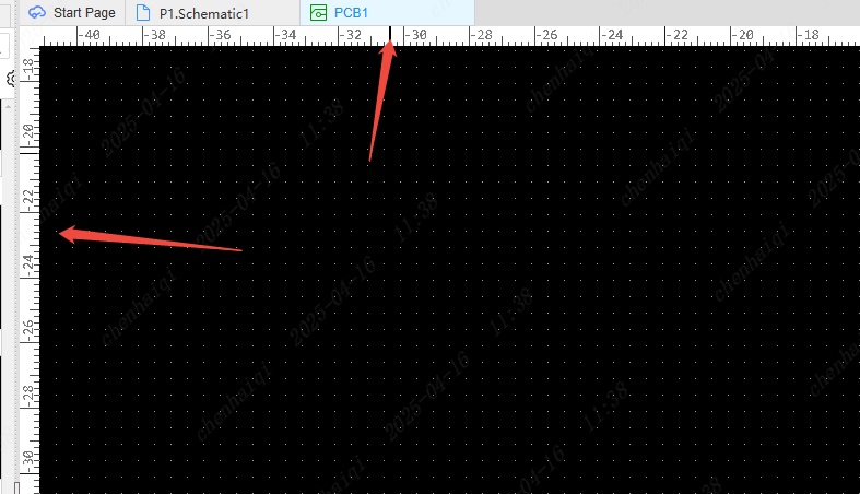
In the top menu bar, you can choose whether to display the scale ruler. 
How to solve the spacing error?
Details
What should I do if a spacing error occurs when checking DRC? Generally speaking, spacing errors are reported because the spacing between elements is too close. We can first check the content of the error report, and then we can clearly see the type of error report as well as the object and content of the error report.  We can take two approaches to solve the spacing error. 1.Manually adjust the spacing between elements.
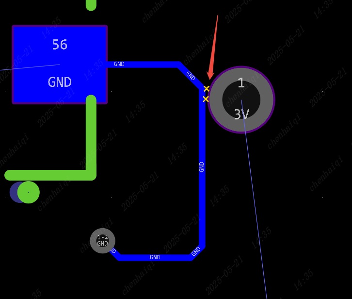
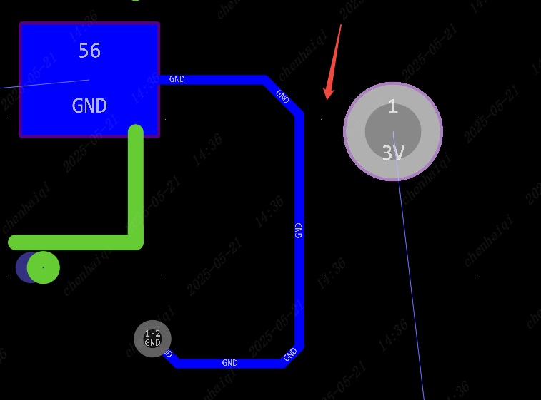 2.Modify the spacing of the design rules.Select the spacing between elements according to the object reporting the error and modify it.
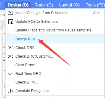
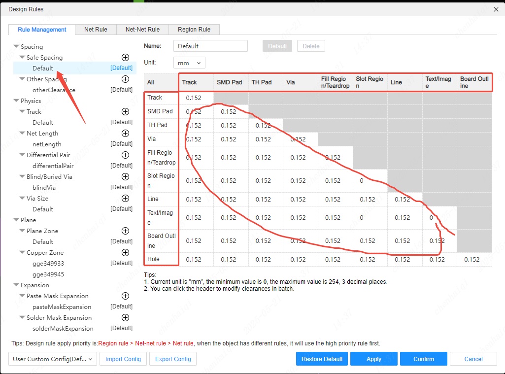
How to solve the error of sub-diagram when modifying design rules?
Details
This is because when the Partition Manager performs the partition deletion operation, the file deletion operation fails, and only the partition record in the canvas is deleted, but the sub-picture partitions PCB is not deleted. 
For this kind of error project, you can only manually delete the sub-picture partitions PCB in the left panel. 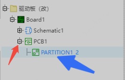
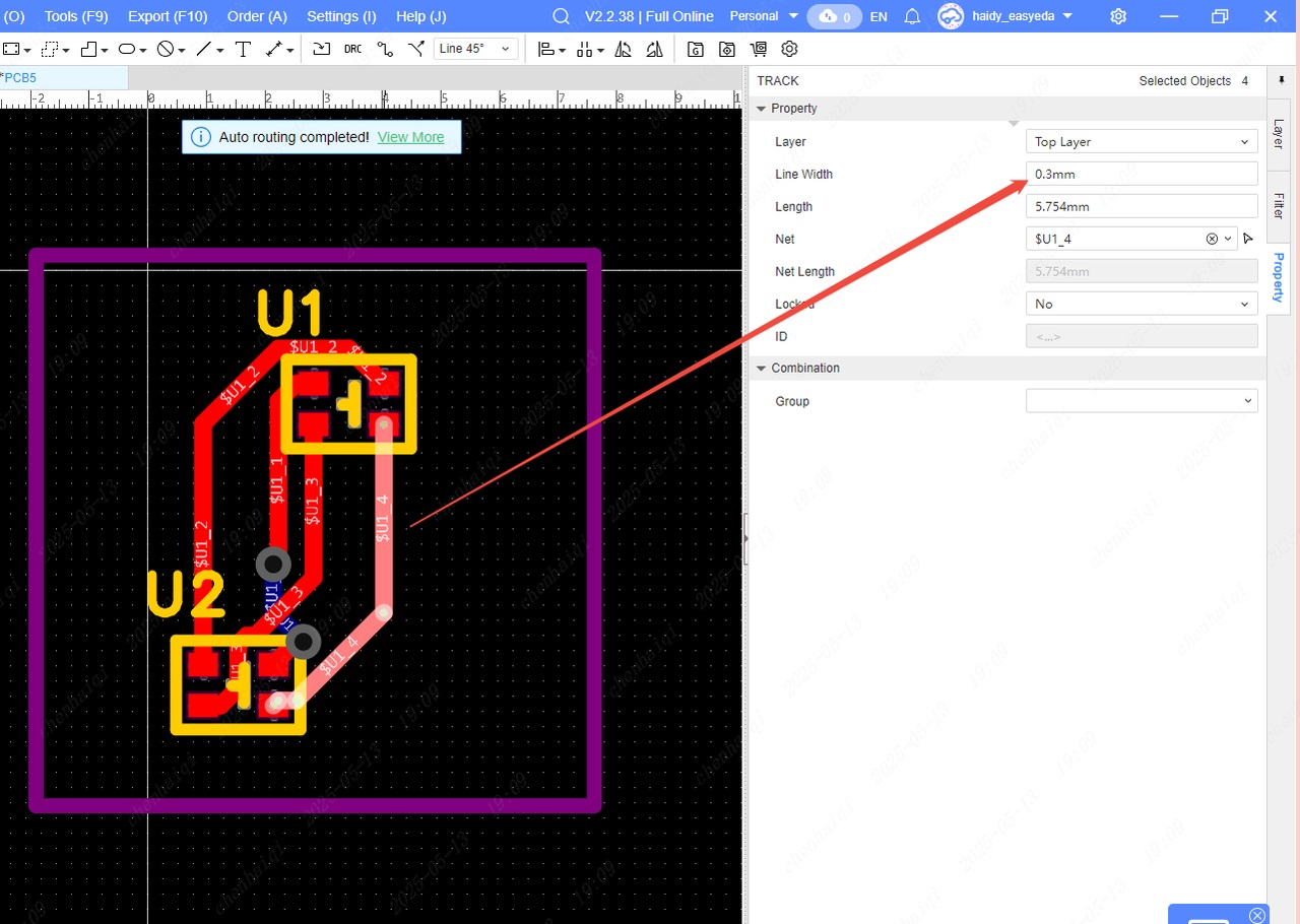
How to modify the routing width of auto route?
Details
First, you need to set "Start Track Width" to "Follow Rule" in the properties. 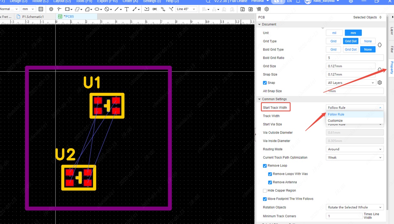
Secondly, modify the wire width rules in the design rules. 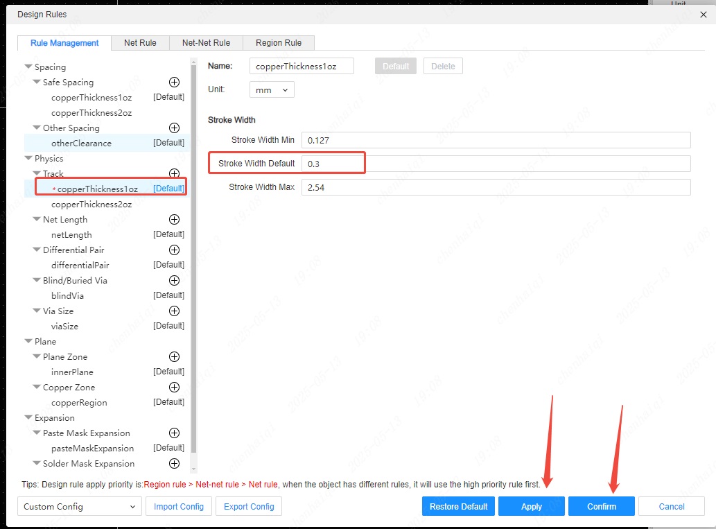
Finally, perform the wiring function. 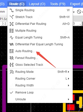
How to set PCB wire to follow the footprint movement?
Details
You can make a selection in the settings in the top menu bar. 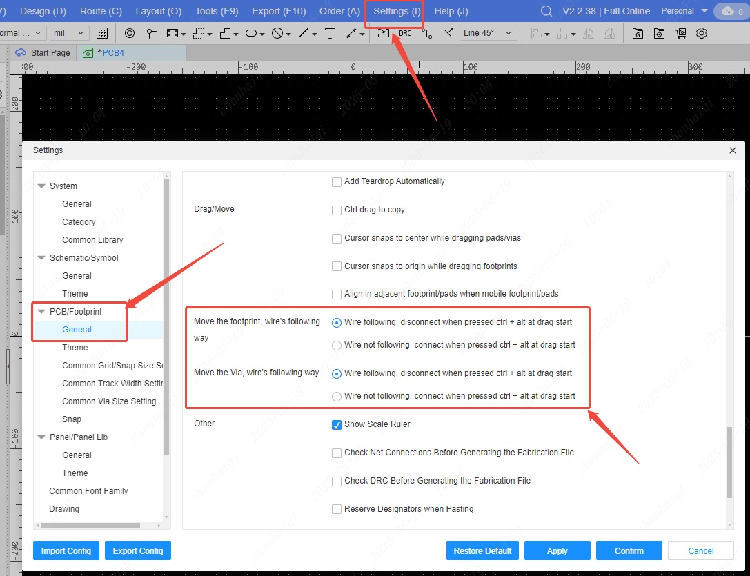
How to batch modify the properties of pads in PCB?
Details
You can check the pad options individually in the "Filter" panel, and then box-select the entire PCB. 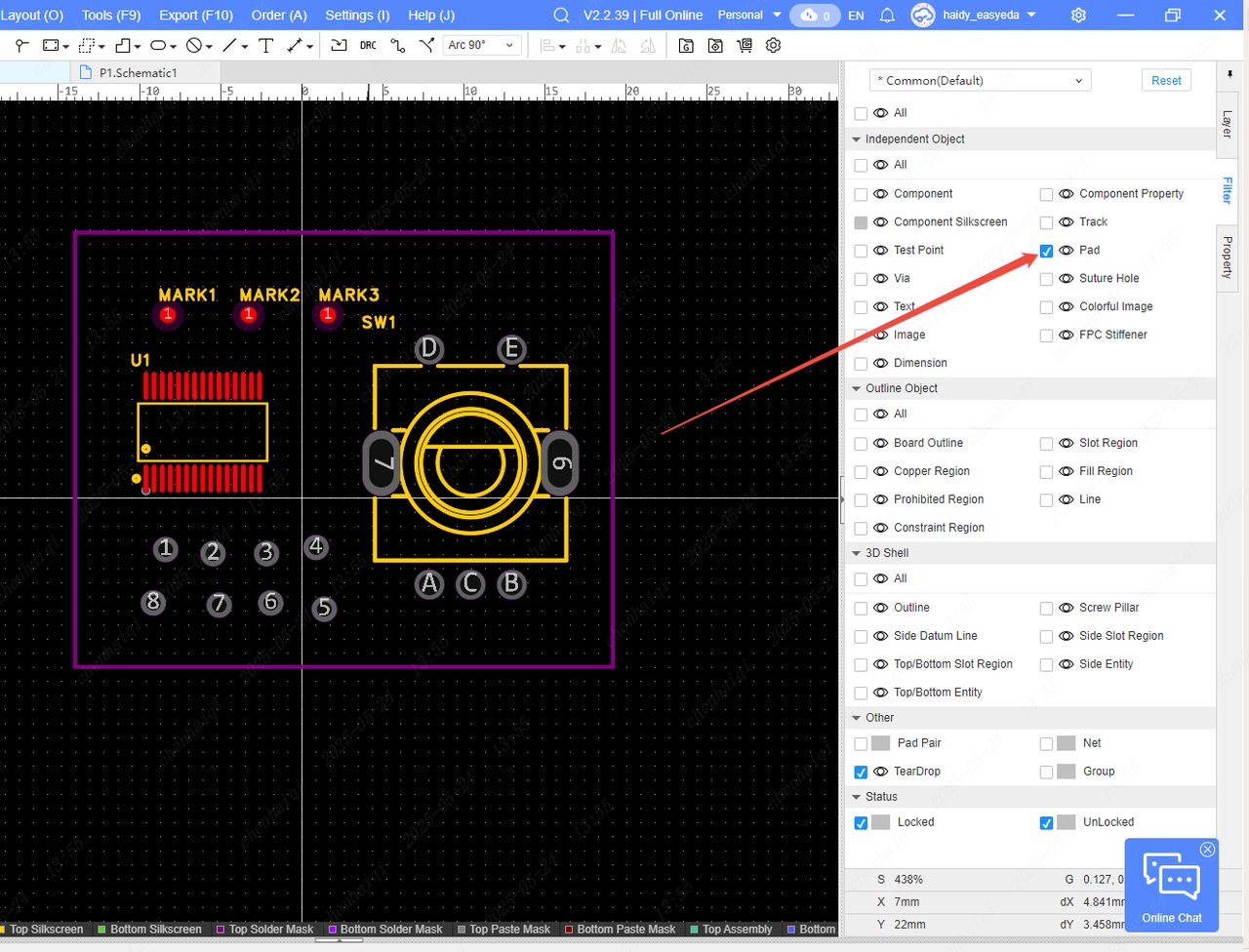
After selecting the box, all pads in the PCB will be selected, whether single-layer or multi-layer. 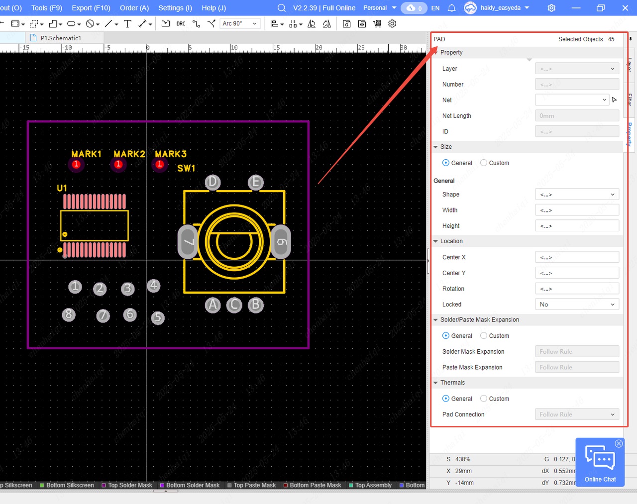
However, it should be noted that since both single-layer pads and multi-layer pads will be selected when selecting pads in batches, not all properties can be selected after selecting. The operation needs to be changed according to the design situation.
Note on USB footprint placement at the edge of the board frame.
Details
When we have some board frame components that need to be placed, we must pay attention to the placement method and design requirements.For example, these three types of devices. 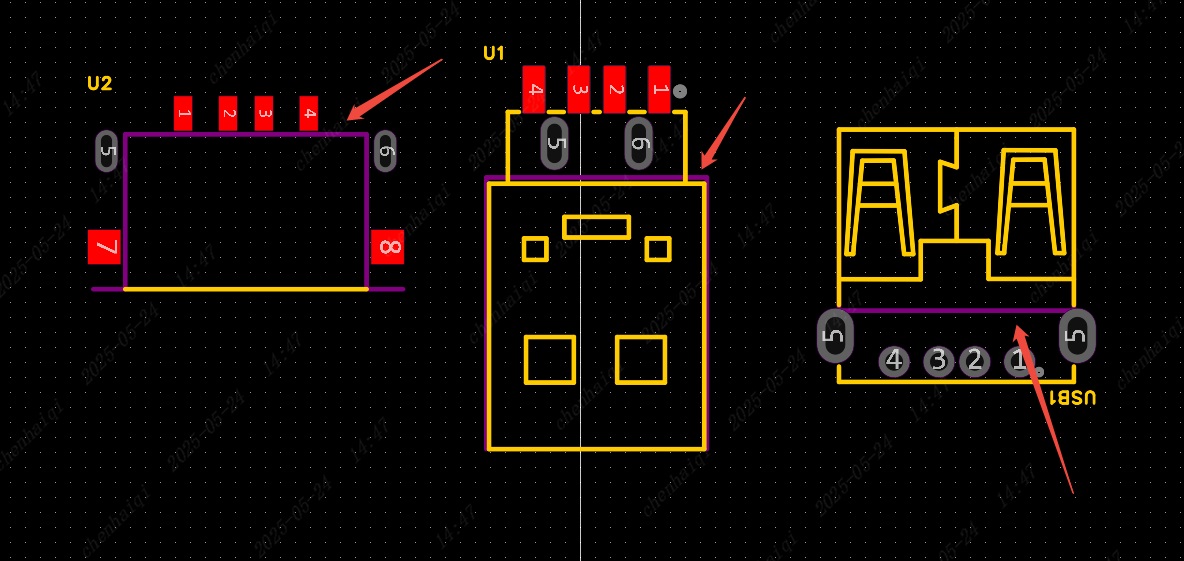 When placing the device, be sure to place it at the position corresponding to the edge of the board and it must be close to the edge of the board.
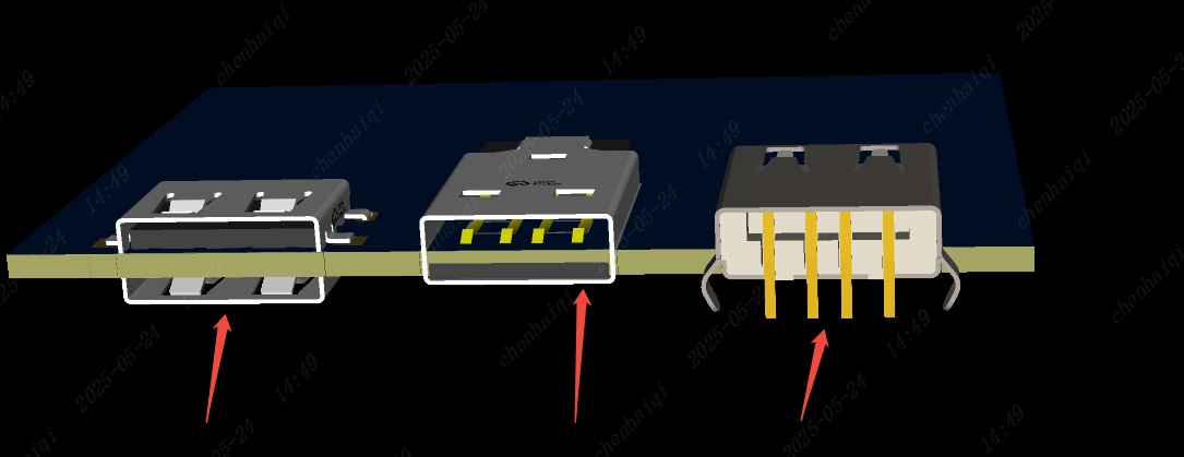
 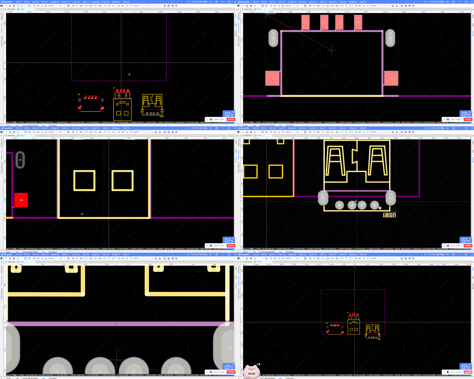 Then you can view the effect in 3D preview.
  However, we also need to pay attention that the frame inside the sinker footprint cannot be in a closed shape with the board frame, otherwise the board will not be grooved, so we need to make some modifications. 1.When it is found that the sinker footprint and the frame are in a closed shape, the frame can be interrupted and deleted
 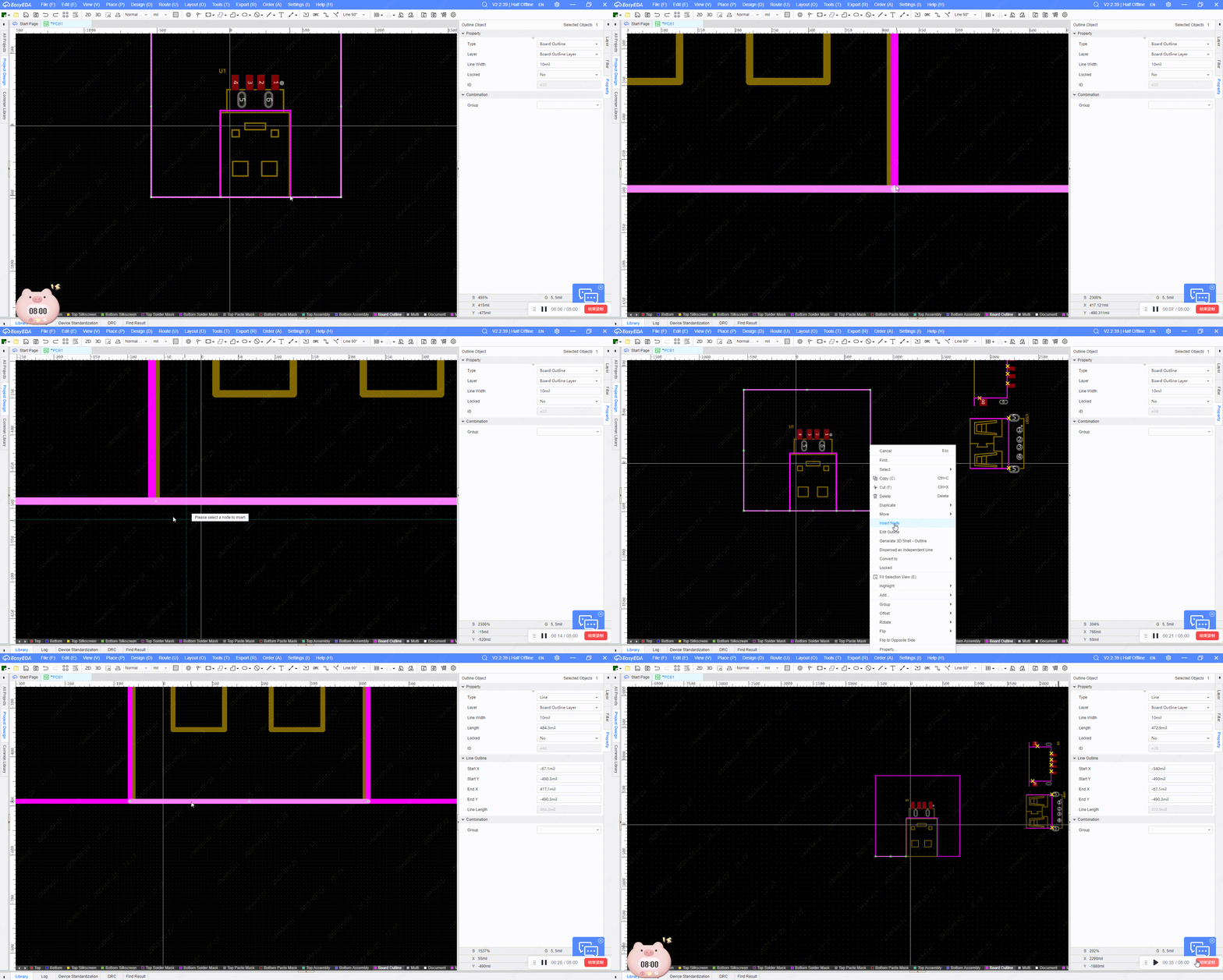 2.Or the frame can be drawn along the footprint with a broken line
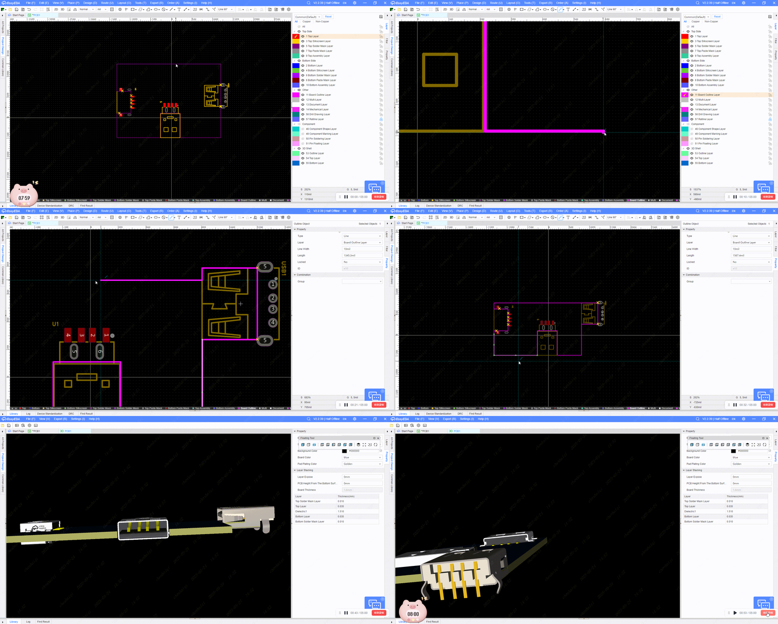
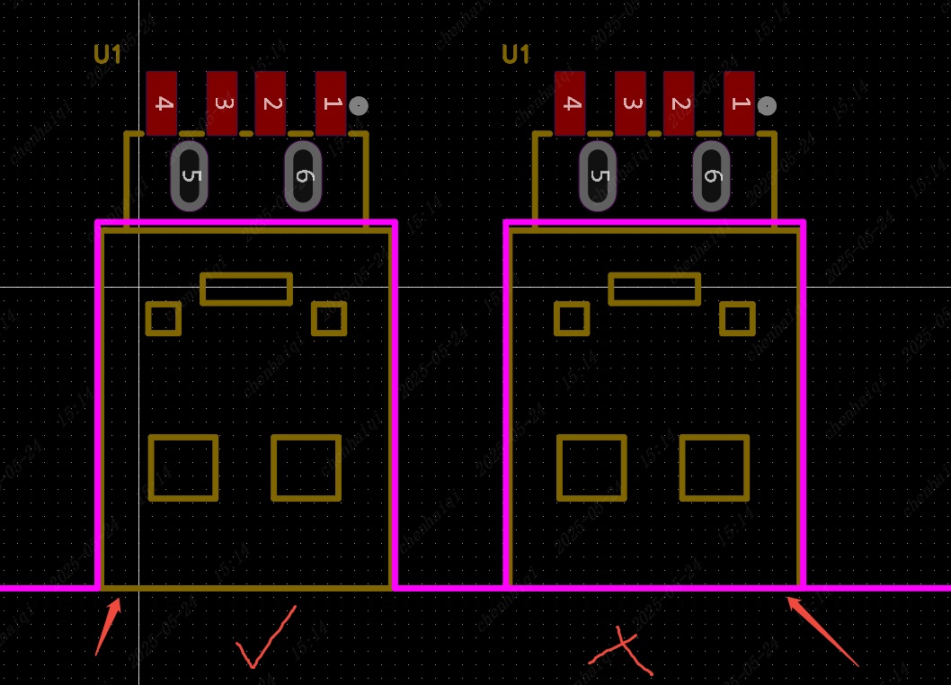
How to set the spacing between different networks and copper plating?
Details
We can achieve different spacing effects between different network elements and copper plating through network-network design rules. For example: My design has two networks, VCC and VDD. I want to place a GND copper area with a different spacing from the two networks. 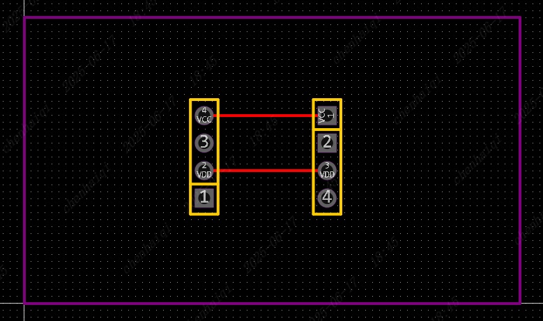
first of all open the design rules and set different spacing rules.Two different spacing rules need to be set in the copper plating rules. 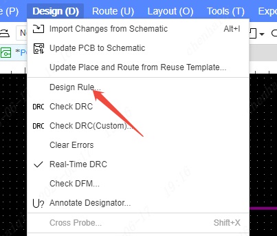
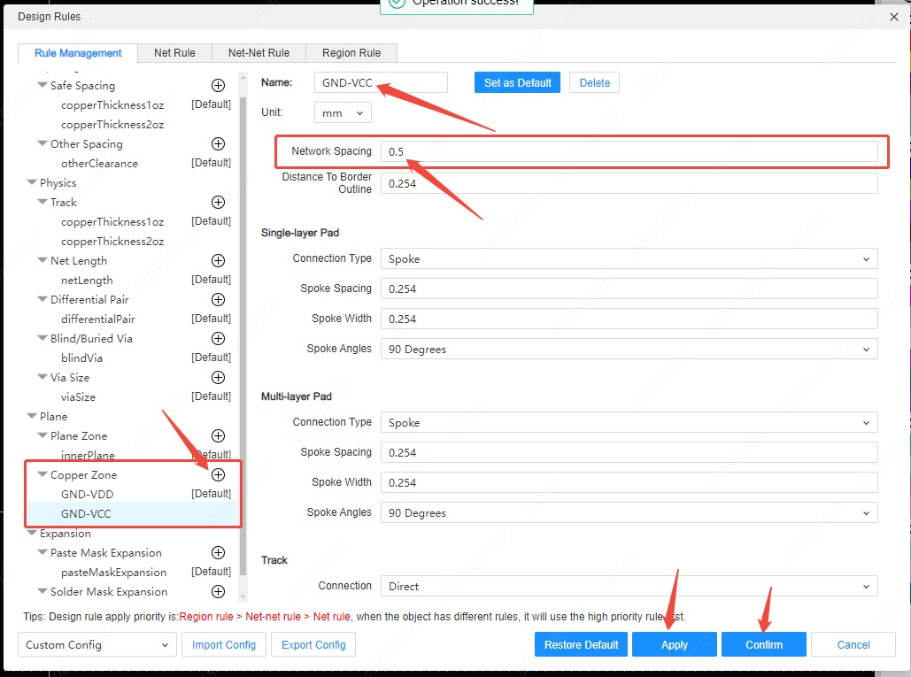
Then click Network-Network Rules to apply the rules to different networks. 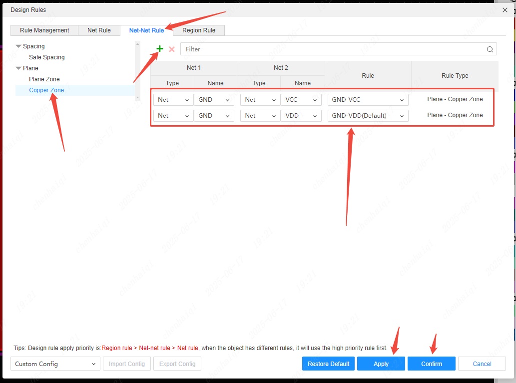
Finally, you can see two different spacings by plating copper. 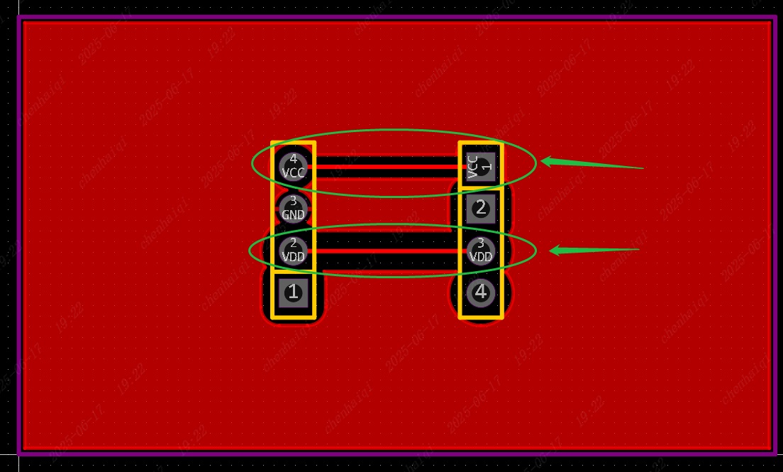
Why can't I select any element on the canvas?
Details
When we cannot select any element on the canvas, we can check whether all are selected in the "Filter" panel on the right. You can also consider this reason when you suddenly cannot select one of the elements. If it is not checked, then elements in the canvas cannot be selected. 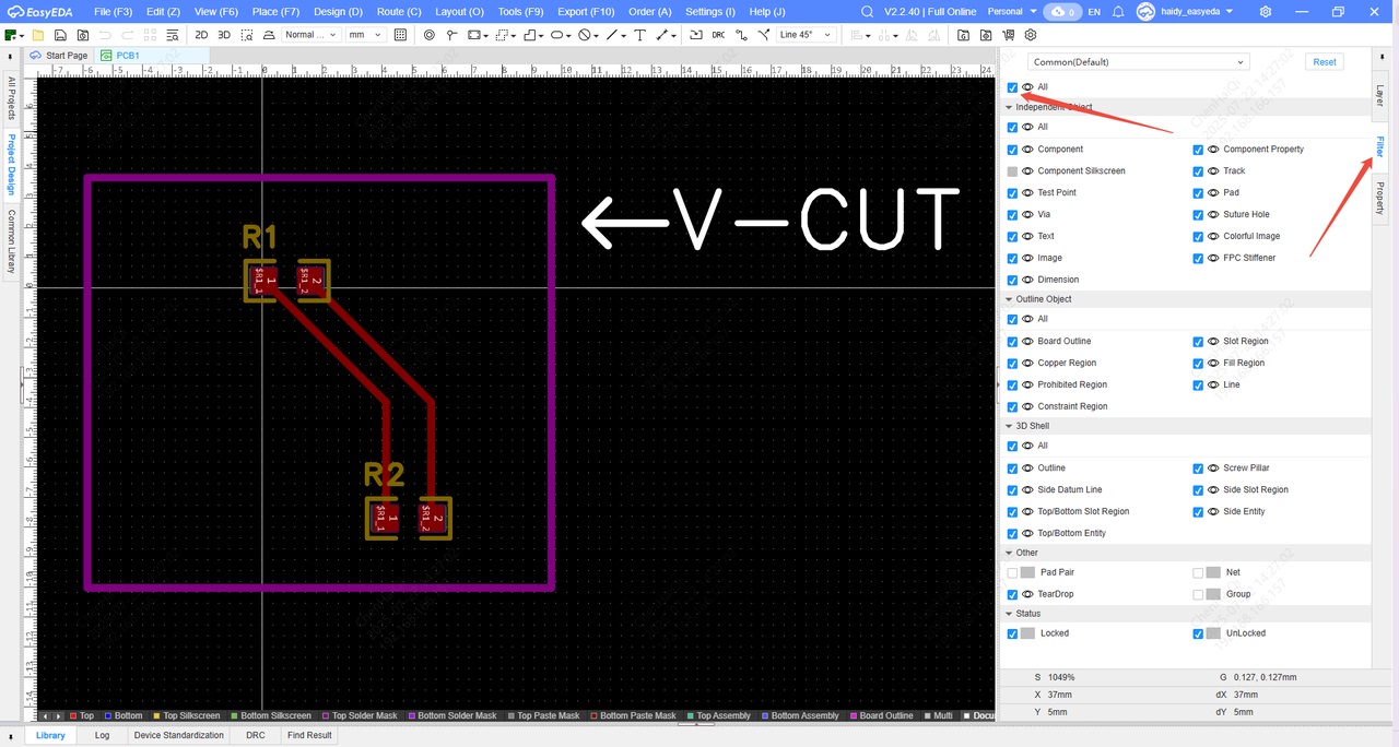
If checking this doesn't work, you can check if the Layers tab is locked.Because the layer is locked, you cannot select all elements of this layer. 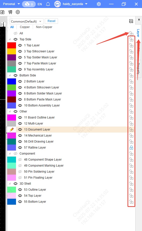
If that doesn't solve the problem you can use the "Unlock All" function to check if any elements are individually locked. 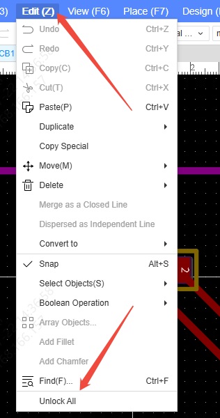
What if you select an element while other elements are selected at the same time?
Details
What should you do if you only want to select one element, but after clicking you find that multiple elements are highlighted at the same time? 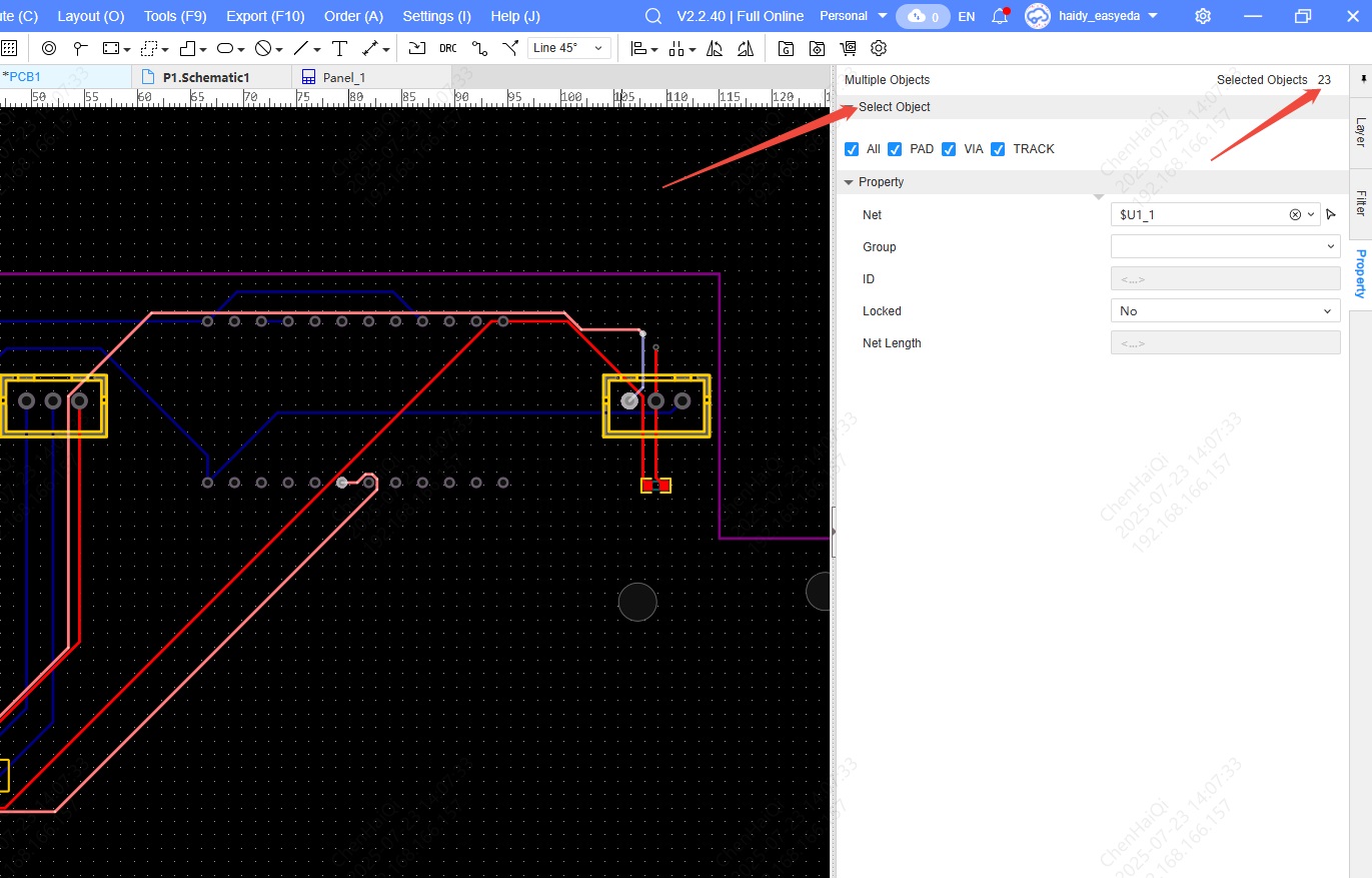
This is because elements of the same network and some elements that are set as group are selected at the same time.You can uncheck the "Pad Pair, Net, Group" and other options in the filter panel on the right. 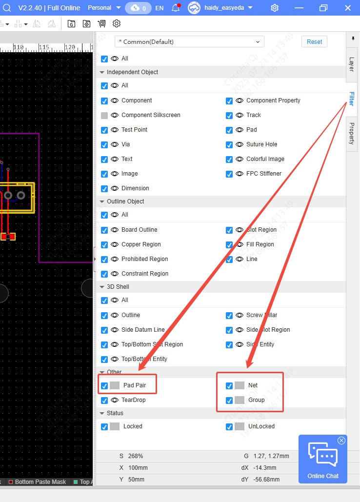
How to modify the wiring angle?
Details
We have six different wiring angles for users to draw wires and lines. You can switch them to the top menu bar or use shortcut keys. 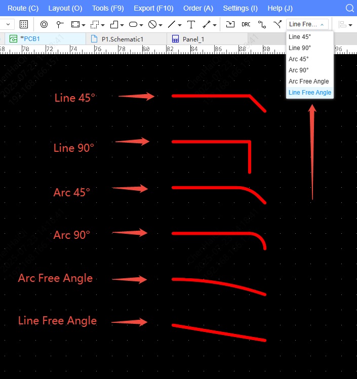

How to change layers using shortcut keys?
Details
You can use the shortcut keys "Alt+T, Alt+B" to switch between the top and bottom layer wiring operations, and the system will automatically place vias for you. 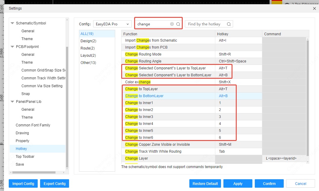
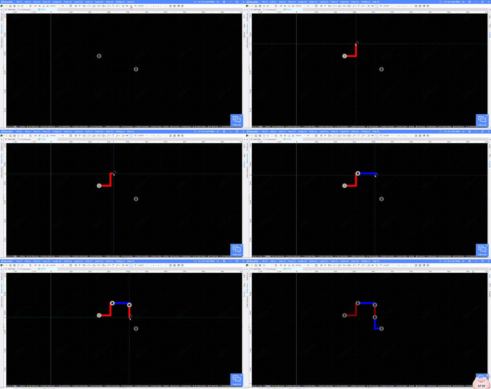
How do I modify the via size on canvas?
Details
There are two ways to modify via hole dimensions. The first is to click on the via and modify it in the properties bar on the right. 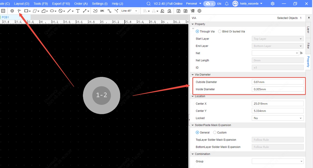
The second method is to enter the design rule interface in the top menu bar and then modify the via size rules. 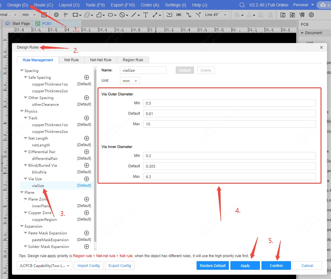
Another tip: in the Properties bar on the left side of the canvas, you can toggle "Start via size" to "Follow the rule or customize." "Follow the rule" means the via will be placed according to the size specified in the design rule. "Customize" allows you to freely modify the via size. Once you change the size after placing a via, subsequent via placements will retain the changed size until you change it again. 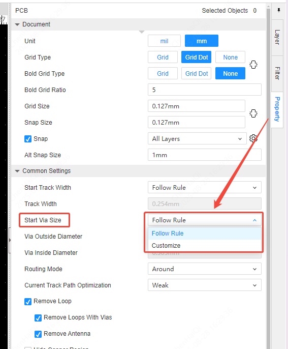
How to modify the divergence linewidth of copper pour?
Details
Spoke Width is generated when the connection method between the copper pour area and the pad is "spoke". The line width of the Spoke Width can be modified. 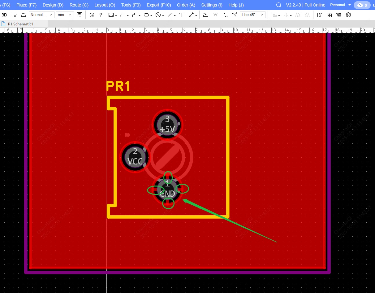
Access the design rules interface from the top menu bar, and then modify the Spoke Width within the copper pour rules. If the modification fails to generate an effect after returning to the PCB interface, remember to use "Shift+B" to rebuild the copper pour. 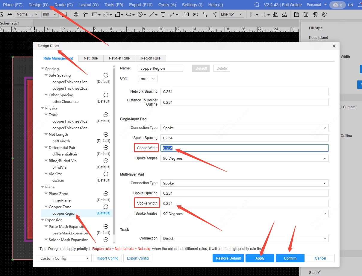 、
、
How to delete a device's 3D model?
Details
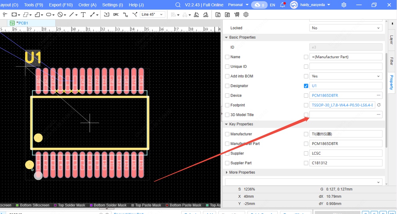
Click on the device, and you will find the 3D model input box at the bottom of the right-hand properties panel. Then click the delete button. 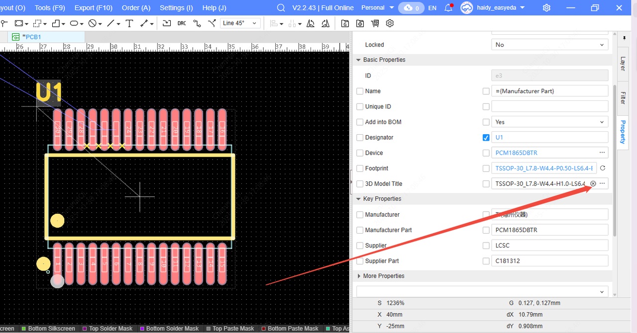
How to resolve the error message "Track DRC violation detected, track could not be generated, please check the white DRC border"?
Details
This error message means that the spacing in some areas is too small, preventing the wires from being pulled out. Therefore, we can change the wiring pattern. 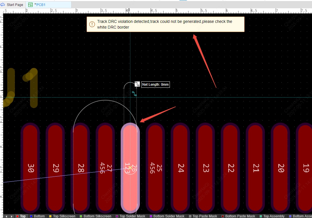
We can temporarily change the wiring mode to "ignore", then pull out the wires with smaller spacing, and then change it back. 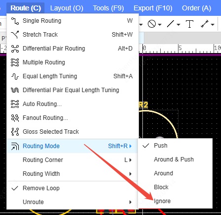
Another method is to try making the traces thinner, or modifying the spacing between pads and between pads and traces in the design rules to smaller values or 0. Note: If you modify the design rules, you must remember to change them back before placing the order to avoid overlooking any errors. 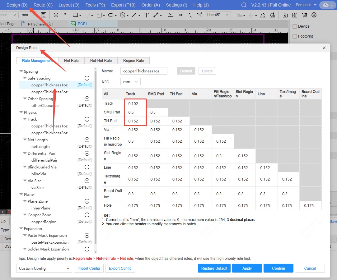
How do I export image files?
Details
To export an image file from a PCB in the professional version, you need to open a 2D preview first and then export a PNG file. 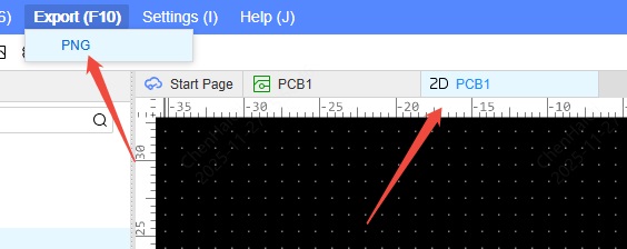
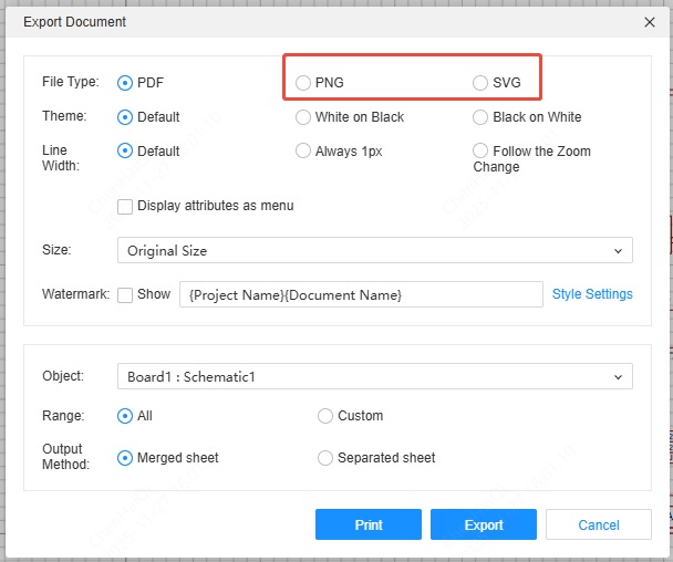
To export the schematic as an image file, you need to select either PNG or SVG file in the top menu bar. 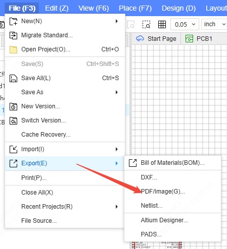
How to use the Copy Special feature?
Details
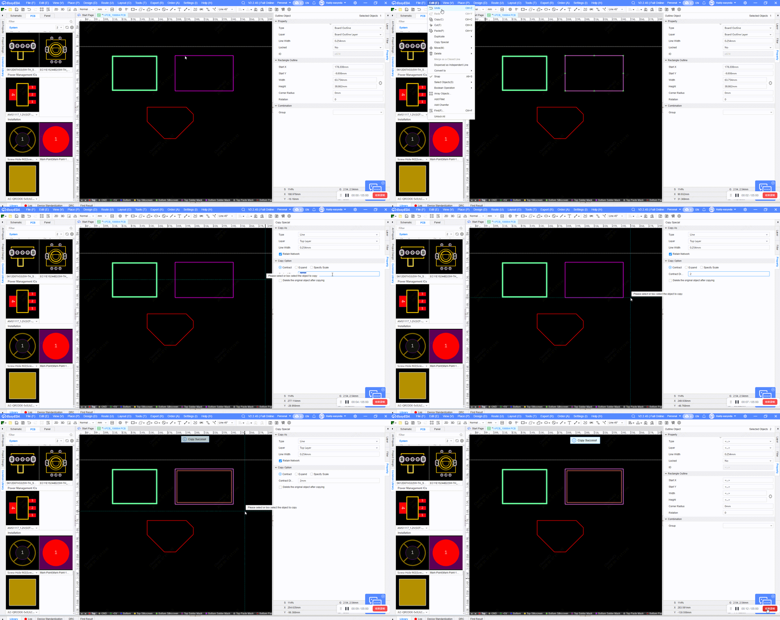
The Copy Special feature can be applied to fully closed elements such as board outlines, 3D shell outlines, and lines. It can also be used with rectangles, circles, and polygons. This feature can be used to zoom in or out on an element. Please note that this cannot be used to enlarge or reduce the size of the entire board and components. Usage steps: 1. Click on the element, and then select the function from the top menu bar. 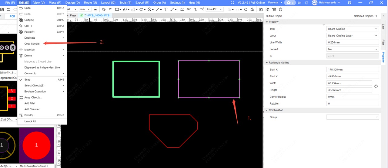
2.Set the parameters in the properties panel on the right, and then select or click the elements that need to be copied. 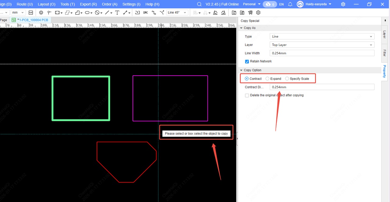
GIF tutorial: 